Low temperature poly-silicon TFT substrate structure and manufacture method thereof

a low temperature polysilicon and substrate technology, applied in the field of display technology, can solve the problems of inability to achieve effective control of the uniformity of the lattice, the uniform crystallization direction of the lattice, and the long distance of the display effect, so as to raise the electron mobility and raise the current uniform

Active Publication Date: 2017-02-02
SHENZHEN CHINA STAR OPTOELECTRONICS TECH CO LTD
View PDF3 Cites 1 Cited by
  • Summary
  • Abstract
  • Description
  • Claims
  • Application Information

AI Technical Summary

Benefits of technology

[0013]An objective of the present invention is to provide a manufacture method of a Low Temperature Poly-silicon TFT substrate structure, capable of controlling the crystallization process of the polysilicon to make that the larger lattice dimension of the polysilicon layer is formed in the drive TFT area in the crystallization process and raise the

Problems solved by technology

However, the ELA crystallization technology according to prior art cannot achieve effective control to the uniformity of the lattices and the crystallization direction of the l

Method used


Image

  • Low temperature poly-silicon TFT substrate structure and manufacture method thereof
  • Low temperature poly-silicon TFT substrate structure and manufacture method thereof
  • Low temperature poly-silicon TFT substrate structure and manufacture method thereof

Examples


Embodiment Construction

[0054]For better explaining the technical solution and the effect of the present invention, the present invention will be further described in detail with the accompanying drawings and the specific embodiments.

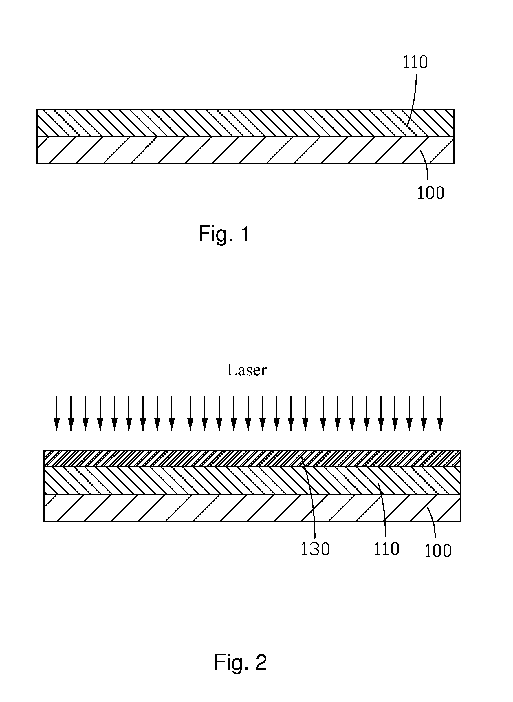
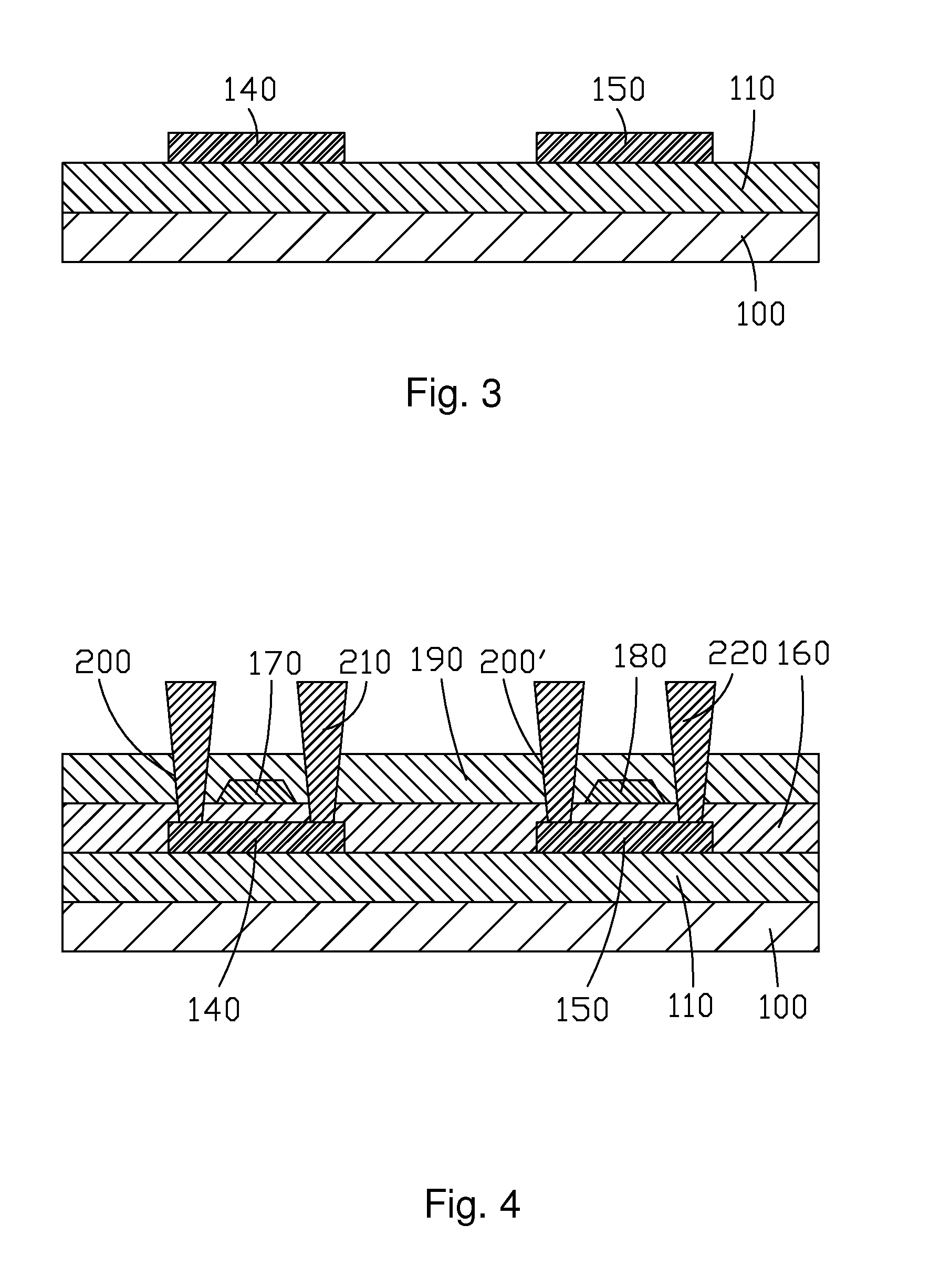
[0055]Please refer to FIG. 5. The present invention first provides a manufacture method of a Low Temperature Poly-silicon TFT substrate structure, comprising steps of:

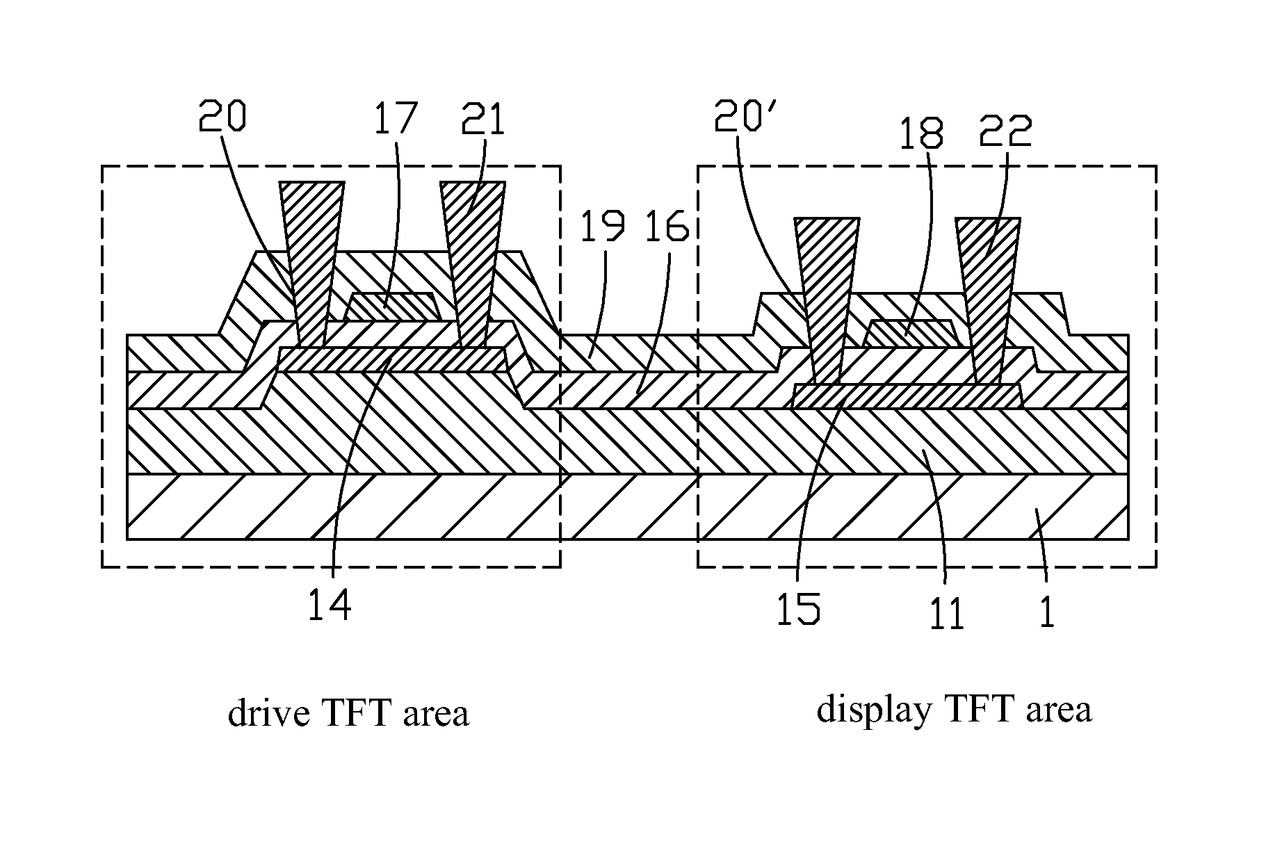
[0056]step 1, as shown in FIGS. 6-7, providing a substrate 1, and the substrate 1 comprises a drive TFT area and a display TFT area, and deposing a buffer layer 11 on the substrate 1, and patterning the buffer layer 11 to make a thickness of the buffer layer 11 in the drive TFT area be larger than a thickness of the buffer layer 11 in the display TFT area;

[0057]specifically, the substrate 1 is a glass substrate, and material of the buffer layer 11 is Silicon Oxide (SiOx), Silicon Nitride (SiNx) or a combination of the two.

[0058]By providing the buffer layers 11 in the drive TFT area and the display TFT area with ...


PUM


Abstract

The present invention provides a Low Temperature Poly-silicon TFT substrate structure and a manufacture method thereof. By providing the buffer layers in the drive TFT area and the display TFT area with different thicknesses, of which the thickness of the buffer layer in the drive TFT area is larger, and the thickness of the buffer layer in the display TFT area is smaller, different temperature grades are formed in the crystallization process of the polysilicon to achieve the control to the grain diameters of the crystals. The polysilicon layer with larger lattice dimension is formed in the drive TFT area in the crystallization process to raise the electron mobility. The fractured crystals of polysilicon layer in the display TFT area can be obtained in the crystallization process for ensuring the uniformity of the grain boundary and raising the uniformity of the current. Accordingly, the electrical property demands for different TFTs can be satisfied to raise the light uniformity of the OLED.

Description

FIELD OF THE INVENTION[0001]The present invention relates to a display technology field, and more particularly to a Low Temperature Poly-silicon TFT substrate structure and a manufacture method thereof.BACKGROUND OF THE INVENTION[0002]The Low Temperature Poly-silicon (LTPS) technology is the manufacture technology of the new generation TFT substrate. The most significant difference from the traditional amorphous silicon (a-Si) is that the response speed of the LTPS display is faster and possesses advantages of high brightness, high resolution and low electrical power consumption. The Poly-silicon (Poly-Si) possesses excellent electrical property, and better drive ability to the Active-Matrix Organic Light Emitting Diode (AMOLED). Thus, the AMOLED display back plate based on the Low Temperature Poly-silicon technology has been widely utilized at present.[0003]The present manufacture method of the LTPS TFT substrate mainly comprises steps of:[0004]step 1, as shown in FIG. 1, providing...

Claims


Application Information

Patent Timeline
IPC IPC(8): H01L27/12H01L29/786
CPCH01L29/78696H01L27/1222H01L27/124H01L29/78675H01L27/3262H01L27/1296H01L27/1274H01L21/268H01L21/77H01L27/12H01L27/1214H10K59/00H01L27/1218H01L27/1281H01L27/1262H10K59/1213
Inventor ZHANG, XIAOXING
Owner SHENZHEN CHINA STAR OPTOELECTRONICS TECH CO LTD
Why Eureka
Try Eureka