Semiconductor device and manufacturing method thereof

Active Publication Date: 2017-02-09
SEMICON ENERGY LAB CO LTD
View PDF1 Cites 11 Cited by
  • Summary
  • Abstract
  • Description
  • Claims
  • Application Information

AI Technical Summary

Benefits of technology

[0028]The threshold voltage of the semiconductor device can be adjusted to an appropriate value. Alternatively, degradation of electrical characteristics of the semiconductor device due to miniaturization can be suppressed.
[0029]A transistor having a high on-state current can be provided. A semiconductor device including a transistor capable of high-speed operation can be provided. A transistor of the present invention can have favorable driving characteristics because of its high on-state current and low off-state current. A transistor with high and stable electrical characterist

Problems solved by technology

Miniaturization of transistors may cause deterioration of the electrical characteristics of the transist

Method used


Image

  • Semiconductor device and manufacturing method thereof
  • Semiconductor device and manufacturing method thereof
  • Semiconductor device and manufacturing method thereof

Examples


embodiment 1

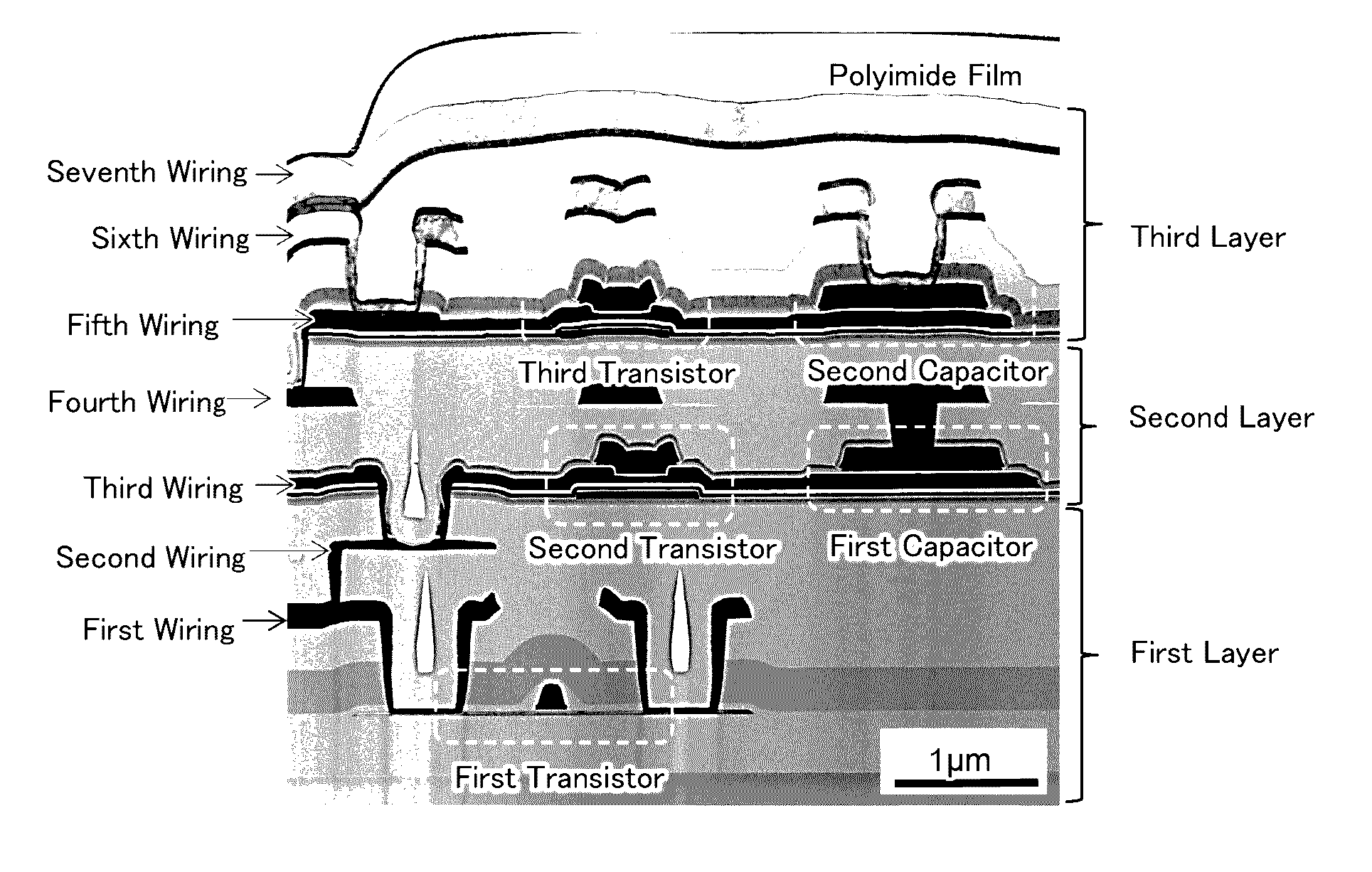
[0095]In this embodiment, one embodiment of a semiconductor device is described with reference to FIG. 1, FIGS. 2A to 2C, FIG. 3, FIGS. 4A and 4B, FIGS. 5A to 5C, FIGS. 6A to 6C, and FIGS. 7A to 7C.

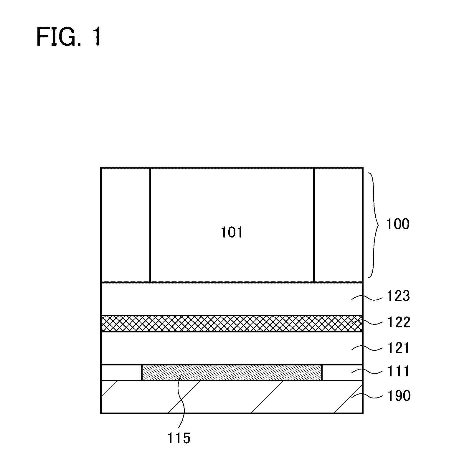
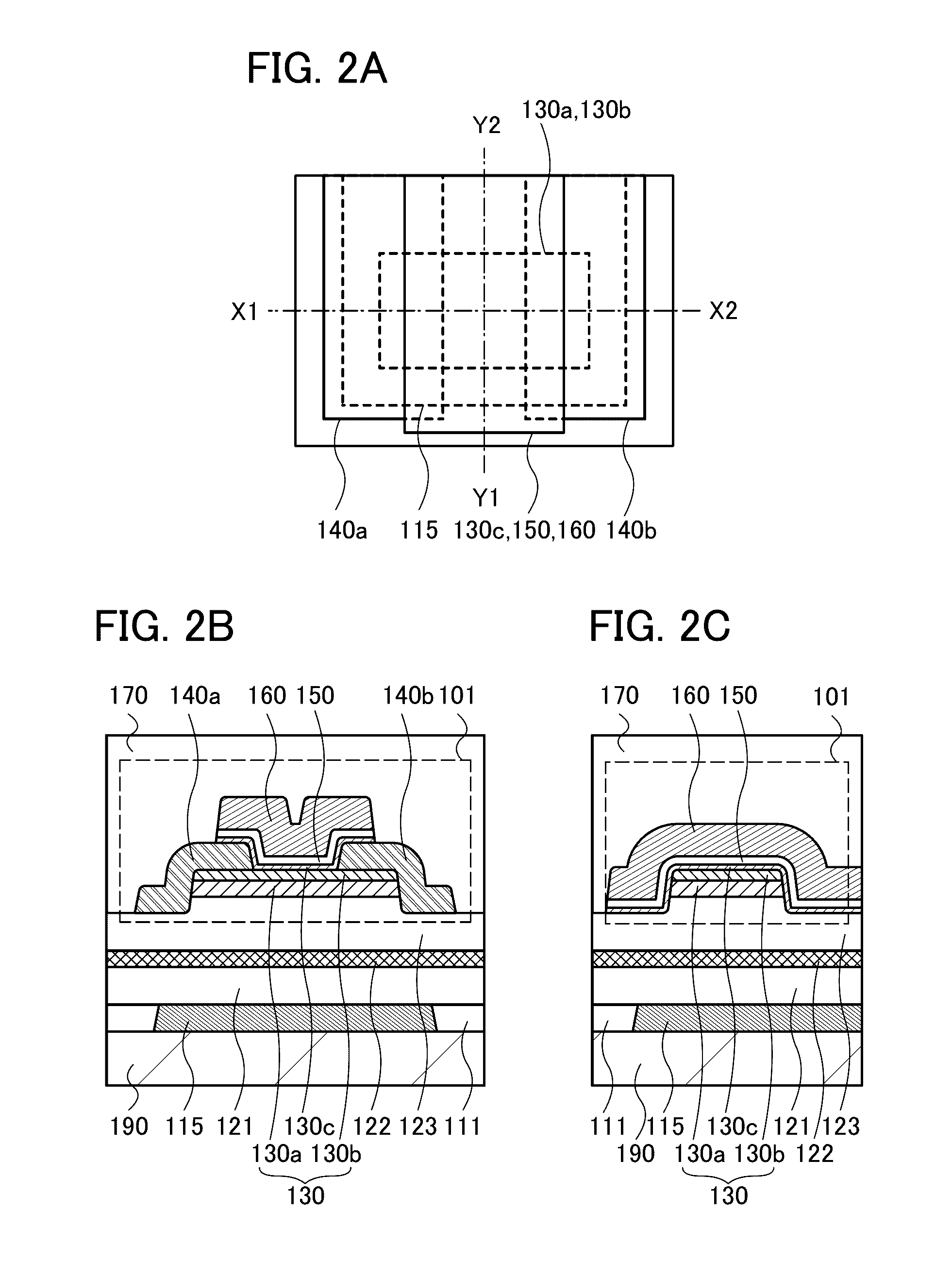
[0096]In this embodiment, a structure of a semiconductor device that includes a layer including a transistor, a first insulator, a fixed charge layer, a second insulator, and a layer including a conductor is described. FIG. 1 illustrates a semiconductor device that includes, over a substrate 190, an insulator 111 including a conductor 115, an insulator 121, a fixed charge layer 122, an insulator 123, and a layer 100 including a transistor 101.

[0097]Since electrons (hereinafter, referred to as fixed charges) exist at an interface between the fixed charge layer 122 and the insulator 123 and an interface between the fixed charge layer 122 and the insulator 121 and inside the fixed charge layer 122, the fixed charge layer 122 is negatively charged. As detailed later, the conductor 115, the in...

embodiment 2

[0172]In this embodiment, one embodiment of a semiconductor device is described with reference to FIGS. 8A and 8B and FIGS. 9A and 9B.

[0173]In this embodiment, a structure of a semiconductor device illustrated in FIG. 8A which includes a layer including a transistor, a first insulator, a fixed charge layer, a second insulator, and a layer including a conductor is described. FIGS. 8A and 8B illustrate a semiconductor device that includes, over the substrate 190, the insulator 111 including the conductor 115, the insulator 121, the fixed charge layer 122, the insulator 123, and the layer 100 including the transistor 101 and a transistor 102.

[0174]Since fixed charges exist at an interface between the fixed charge layer 122 and the insulator 123 and an interface between the fixed charge layer 122 and the insulator 121 and inside the fixed charge layer 122, the fixed charge layer 122 is negatively charged. Thus, the conductor 115, a region of the insulator 121 which overlaps with the con...

embodiment 3

[0197]In this embodiment, one embodiment of a semiconductor device is described with reference to FIG. 10 and FIGS. 11A to 11C.

[0198]In this embodiment, a structure of a semiconductor device illustrated in FIG. 10 which includes a layer including a transistor, a first insulator, a fixed charge layer, a second insulator, and a layer including a conductor is described. Note that in the semiconductor device illustrated in FIG. 10, components having the same functions as the components in the semiconductor device illustrated in FIG. 8A are denoted by the same reference numerals.

[0199]FIG. 10 illustrates a semiconductor device that includes, over the substrate 190, the insulator 111 including the conductor 116, an insulator 112, an insulator 113 including the conductor 115, the insulator 121, the fixed charge layer 122, the insulator 123, and the layer 100 including the transistors 101 and 102.

[0200]Note that in the structure, the total thickness of the insulators between the transistor ...


PUM


Abstract

A miniaturized transistor with reduced parasitic capacitance and highly stable electrical characteristics is provided. High performance and high reliability of a semiconductor device including the transistor is achieved. A first conductor is formed over a substrate, a first insulator is formed over the first conductor, a layer that retains fixed charges is formed over the first insulator, a second insulator is formed over the layer that retains fixed charges, and a transistor is formed over the second insulator. Threshold voltage Vth is controlled by appropriate adjustment of the thicknesses of the first insulator, the second insulator, and the layer that retains fixed charges.

Description

BACKGROUND OF THE INVENTION[0001]1. Field of the Invention[0002]The present invention relates to, for example, an oxide, a transistor, a semiconductor device, and manufacturing methods thereof. The present invention relates to, for example, an oxide, a display device, a light-emitting device, a lighting device, a power storage device, a memory device, a processor, an imaging device, and an electronic device. The present invention relates to methods for manufacturing an oxide, a display device, a liquid crystal display device, a light-emitting device, a memory device, a processor, an imaging device, and an electronic device. The present invention relates to methods for driving a semiconductor device, a display device, a liquid crystal display device, a light-emitting device, a memory device, a processor, an imaging device, and an electronic device.[0003]Note that one embodiment of the present invention is not limited to the above technical field. The technical field of one embodiment...

Claims


Application Information

Patent Timeline
IPC IPC(8): H01L29/40H01L49/02H01L27/06
CPCH01L29/408H01L28/60H01L27/0629H01L21/8258H01L27/0688H01L29/78648H01L29/78696H01L27/1225H01L27/1251H01L28/00H01L23/5223H01L27/1207H01L27/1255
Inventor TANAKA, TETSUHIROTANEMURA, KAZUKIMATSUBAYASHI, DAISUKE
Owner SEMICON ENERGY LAB CO LTD
Why Eureka
Try Eureka