Approach for an Area-Efficient and Scalable CMOS Performance Based on Advanced Silicon-On-Insulator (SOI), Silicon-On-Sapphire (SOS) and Silicon-On-Nothing (SON) Technologies

Inactive Publication Date: 2017-02-09
TARAKJI AHMAD
View PDF0 Cites 7 Cited by
  • Summary
  • Abstract
  • Description
  • Claims
  • Application Information

AI Technical Summary

Benefits of technology

[0071]FIG. 9: Measured and simulated Current-Voltage transfer curves of FD-SOI NMOS devices (WGeff=2 μm; LG=0.35 μm; VDS=3.6V (VDS is the applied Potential to the Drain); Box=0.5 μm; CFox-10 nm; tsi=35 nm). Clearly shown is the Bipolar effect in a device that failed to maintain a voltage drop throughout its P_Pocket below the typical diode-drop.
[0072]FIG. 10: Measured and simulated Subthreshold-Slope (SS), from 3D TCAD, in our optimized FD SOI NMOS of FIG. 9 (WGeff=2 μm; LG=0.35 μm; VDS=3.6V; B

Problems solved by technology

No such approach was defined or demonstrated prior from other inventors in the field, and no products have been commercialized to date based on any of the SOI, SOS or SO

Method used


Image

  • Approach for an Area-Efficient and Scalable CMOS Performance Based on Advanced Silicon-On-Insulator (SOI), Silicon-On-Sapphire (SOS) and Silicon-On-Nothing (SON) Technologies
  • Approach for an Area-Efficient and Scalable CMOS Performance Based on Advanced Silicon-On-Insulator (SOI), Silicon-On-Sapphire (SOS) and Silicon-On-Nothing (SON) Technologies
  • Approach for an Area-Efficient and Scalable CMOS Performance Based on Advanced Silicon-On-Insulator (SOI), Silicon-On-Sapphire (SOS) and Silicon-On-Nothing (SON) Technologies

Examples


Embodiment Construction

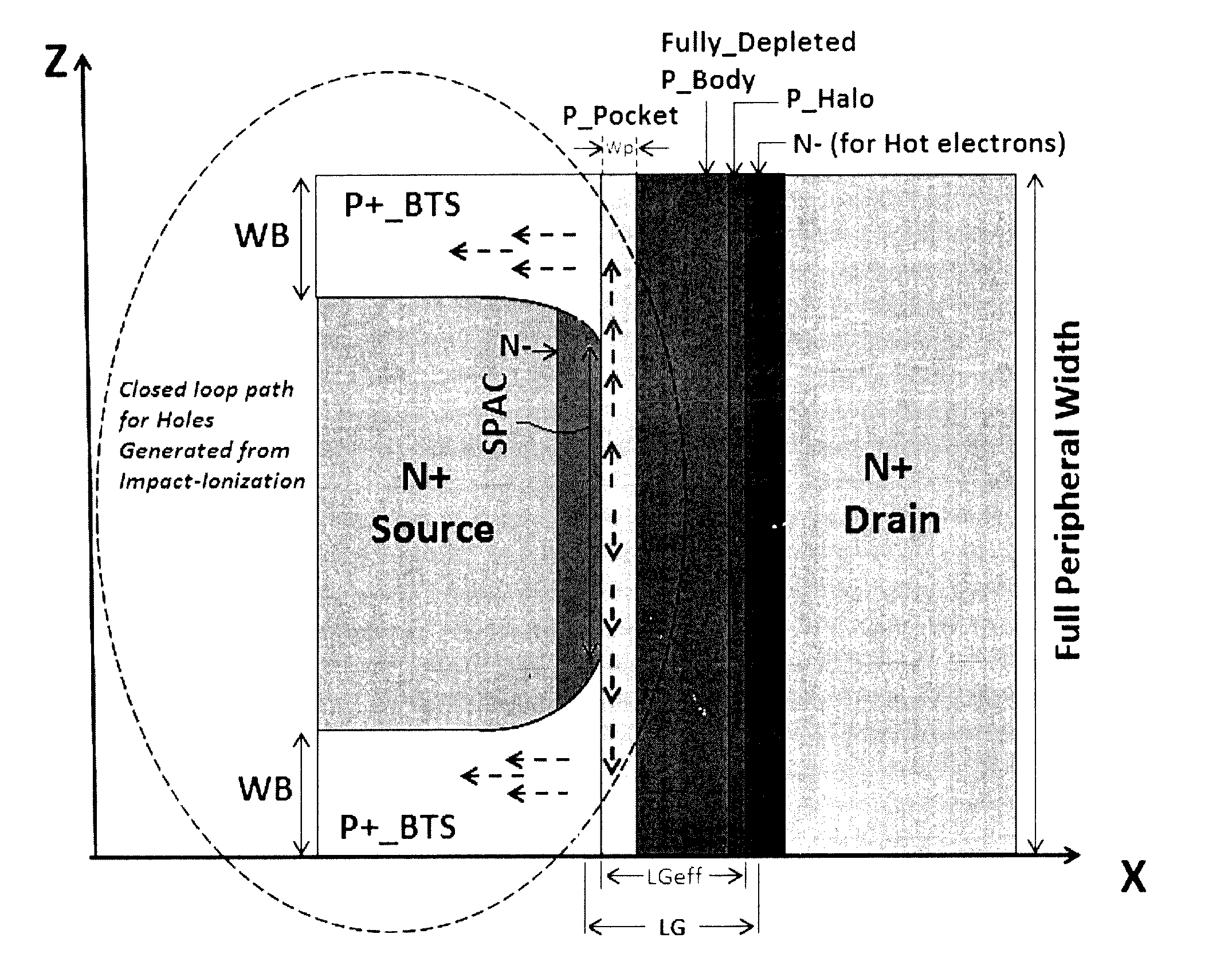
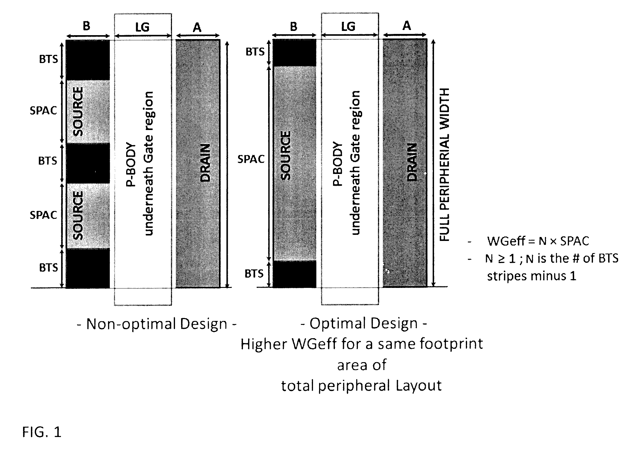
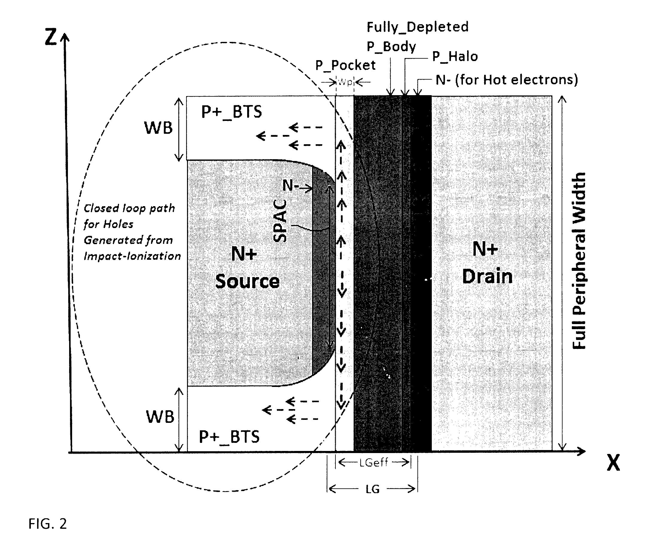
[0074]Today, the total Silicon area consumed by BTS in an IC based on SOI (and similarly based on either the SOS or the SON) is being determined through trial-and-errors such to ensure a fully functional IC that meets some targeted specifications. Consequently, such un-optimized total area of BTS in the IC does lead to larger peripheral footprint of the layout that is not necessary needed. That is not to mention the added time and the higher manufacturing costs that are associated with such repetitive trial-and-errors routines.

[0075]Our well defined and demonstrated design methodology and that is being claimed through this patent application, relies on our unique and proprietary architecture of the 1-legged SOI MOS basis device of FIG. 2, FIG. 3 A, FIG. 3 B and FIG. 3 C that accommodates our design methodology. Our proprietary basis structure is distinct through the tunable (calculated) dimension (Wp) of its P_Pocket alongside the Gate-length, through its analytically defined (calcu...


PUM


Abstract

The invention provides the guided design approach to optimize the device performance for a best area-efficient layout footprint in a single-leg MOS device that is based on any of the SOI, SOS or SON technologies. The design methodology depends on a new proprietary device architecture that is also being claimed in this patent and that allows the implementations of the design equations of our methodology.

Description

INDEX TERMS[0001]CMOS: Complimentary-Metal-Oxide-Semiconductor.[0002]MOS: Metal-Oxide-Semiconductor.[0003]NMOS: N-channel MOS.[0004]PMOS: P-channel MOS.[0005]SOI: Silicon-On-Insulator.[0006]SOS: Silicon-On-Sapphire.[0007]SON: Silicon-On-Nothing.[0008]PD: Partially-Depleted.[0009]FD: Fully-Depleted.[0010]BTS: Body-Tied-Source.[0011]FBE: Floating-Body-Effect.[0012]RF: Radio-Frequency.REFERENCE TO SEQUENCE LISTINGOther Publications[0013][1]. Randy Wolf, Dawn Wang, Alvin Joseph, Alan Botula, Peter Rabbeni, David Harame and Jim Dunn, “Highly Resistive Substrate CMOS on SOI for Wireless Front-End Switch Application”, CS MANTECH Conference, May 16-19, 2011, Palm Springs, Calif., USA.[0014][2]. Cui Jie, Chen Lei, Zhao Peng, Niu Xu, and Liu Yi, “A linear 180 nm SOI CMOS antenna switch module using integrated passive device filters for cellular applications”, Journal of Semiconductors, vo. 35, no. 6, June 2014.[0015][3]. Matteo Maria Vignetti, Michael Salter, Duncan Platt, Anders Hallen, “The...

Claims


Application Information

Patent Timeline
IPC IPC(8): H01L29/786H01L29/78
CPCH01L29/78615H01L29/78603H01L29/78696H01L29/7838H01L29/78612H01L29/78618H01L29/78648H01L27/1203
Inventor TARAKJI, AHMAD
Owner TARAKJI AHMAD
Why Eureka
Try Eureka