Low voltage high density trench-gated power device with uniformly doped channel and its edge termination technique

a high-density, trench-gated technology, applied in the direction of semiconductor devices, electrical devices, transistors, etc., can solve the problems of high channel leakage current, poor high-temperature performance, and device susceptible to punch-through breakdown

Inactive Publication Date: 2003-11-06
SEMICON COMPONENTS IND LLC
View PDF5 Cites 19 Cited by
  • Summary
  • Abstract
  • Description
  • Claims
  • Application Information

AI Technical Summary

Problems solved by technology

This approach achieves a low gate rating, but it may result in a high channel leakage current and a poor high-temperature performance.
Due to the low total net charges of the well, this approach also makes the device susceptible to punch-through breakdown.
In addition, the doping in the channel is non-uniform.
Unfortunately, the non-merging condition imposed on the drift regions 25 as taught in the prior art limits the minimum cell pitch and maximum channel density that the device can employ.
As the result, the on-resistance of the prior art is high when used for a low voltage application.
In addit

Method used


Image

  • Low voltage high density trench-gated power device with uniformly doped channel and its edge termination technique
  • Low voltage high density trench-gated power device with uniformly doped channel and its edge termination technique
  • Low voltage high density trench-gated power device with uniformly doped channel and its edge termination technique

Examples


Embodiment Construction

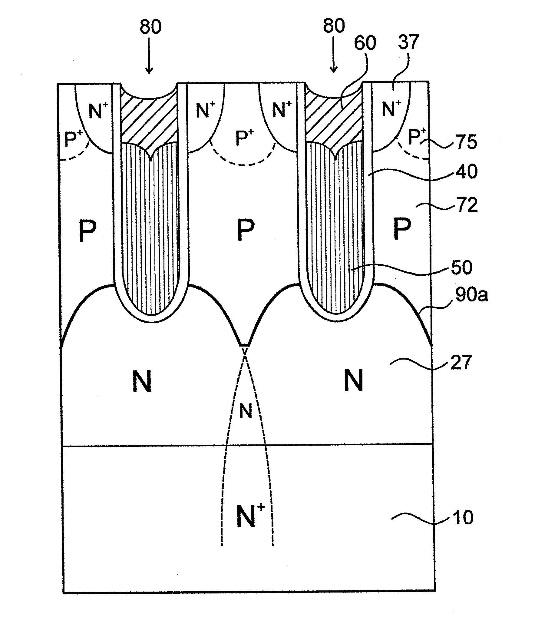
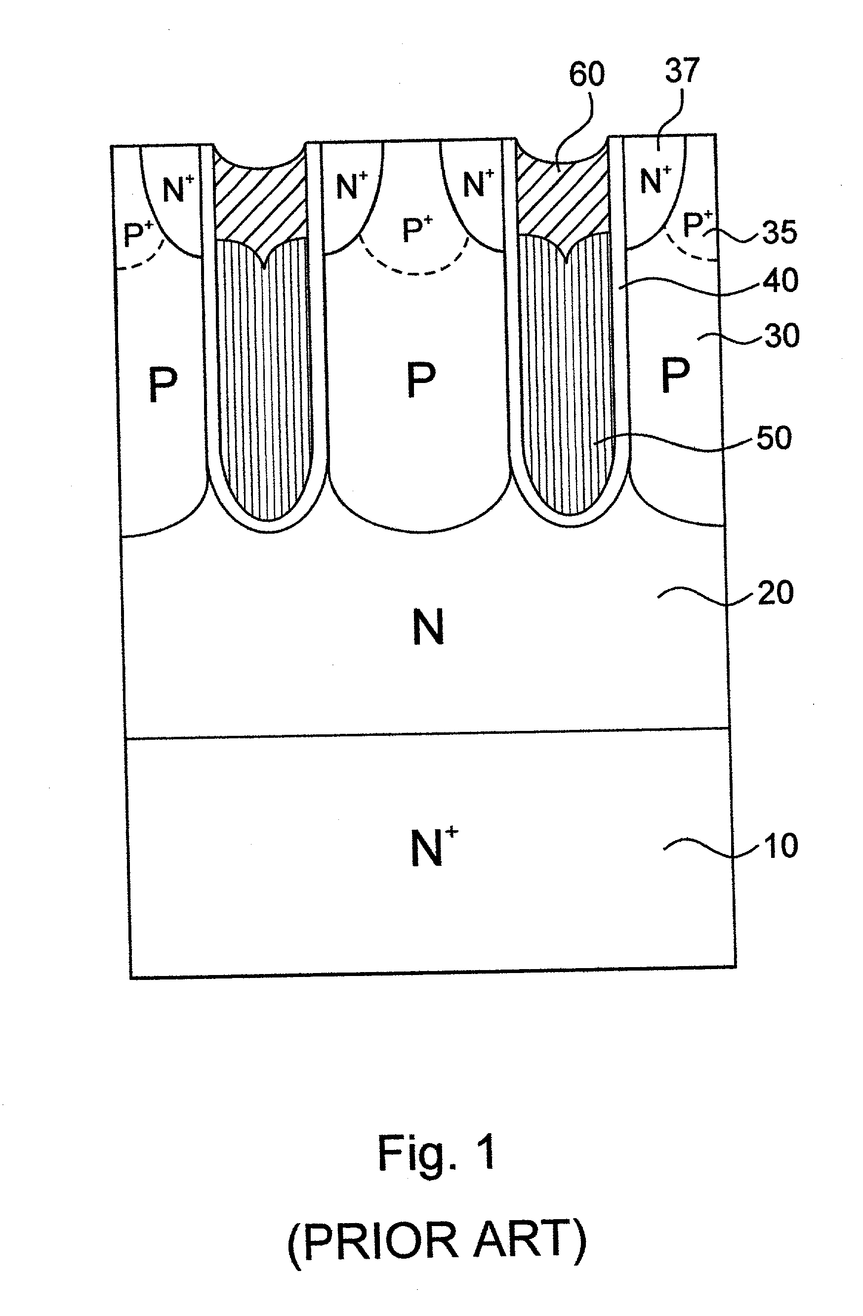
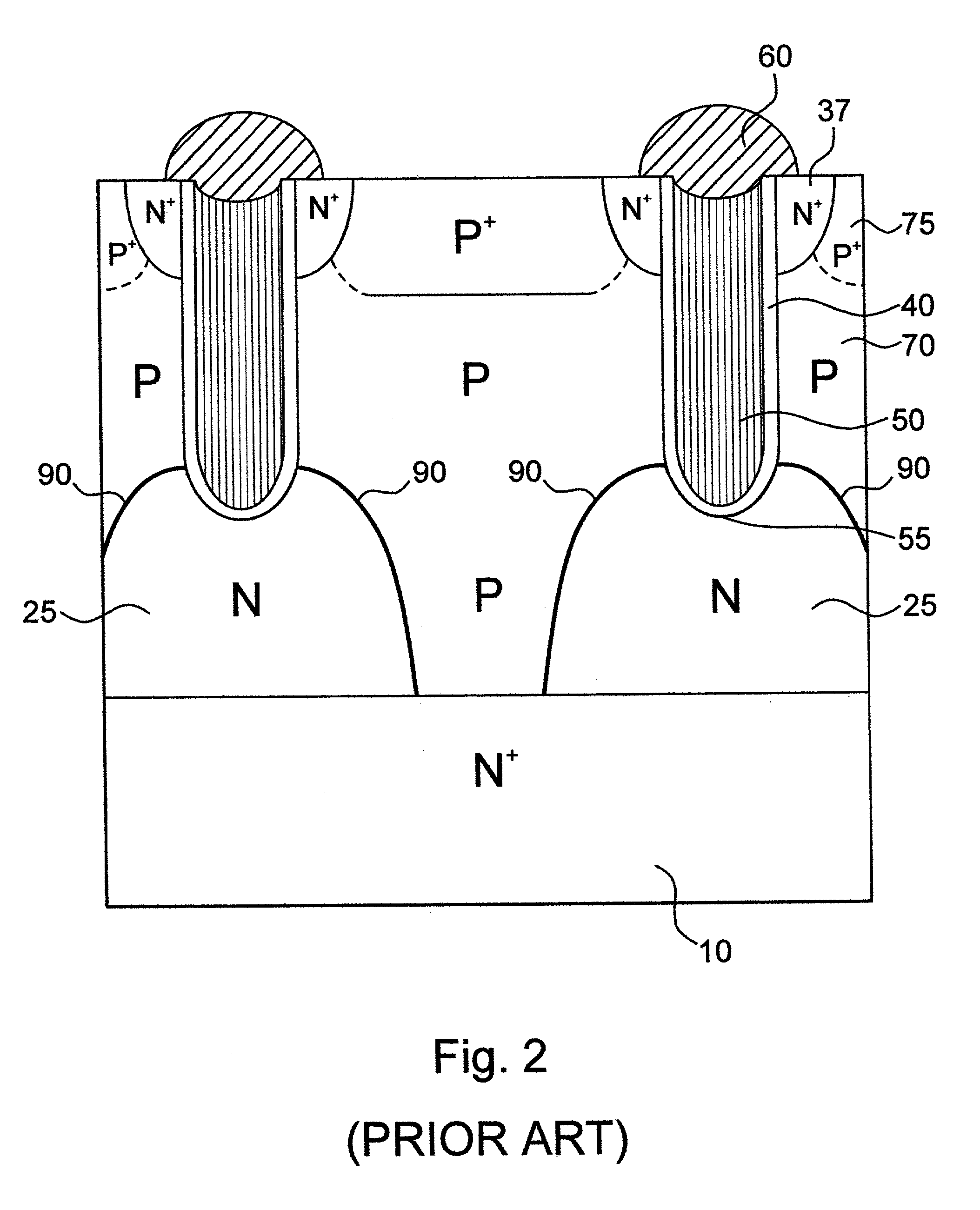
[0019] This invention addresses and resolves the problems of the prior art devices described above. See FIG. 3. The invention's device comprises an N.sup.+-type substrate 10, N-type drift regions 27, a P-type epi-layer 72, trenches 80, gate oxide 40, polysilicon 50, BPSG 60, N.sup.+-type source regions 37, and P.sup.+-type body regions 75. The illustrated conductivity types may of course be reversed as needed. By contrast with the prior art, the invention merges together the implanted drift regions 27. The prior art of FIG. 2 keeps the regions separated to provide a bulk resurf effect that lowers the on resistance and increases the depletion of the drift region during reverse votage conditions to raise the limits of the sustaining reverse voltage. Instead of the long, slanted boundary 90 between P-type epi-layer 70 and drift region 25 as shown in FIG. 2, the invention produces a shorter, more-level boundary 90a between P-type epi-layer 72 and drift region 27 as shown in FIG. 3. In e...


PUM


Abstract

Merging together the drift regions in a low-power trench MOSFET device via a dopant implant through the bottom of the trench permits use of a very small cell pitch, resulting in a very high channel density and a uniformly doped channel and a consequent significant reduction in the channel resistance. By properly choosing the implant dose and the annealing parameters of the drift region, the channel length of the device can be closely controlled, and the channel doping may be made highly uniform. In comparison with a conventional device, the threshold voltage is reduced, the channel resistance is lowered, and the drift region on-resistance is also lowered. Implementing the merged drift regions requires incorporation of a new edge termination design, so that the PN junction formed by the P epi-layer and the N<+> substrate can be terminated at the edge of the die.

Description

[0001] This invention relates to semiconductor power devices and their fabrication, and more specifically to low-voltage vertical MOSFET power devices.DISCUSSION OF PRIOR ART[0002] Recently, the personal portable electronics field, including such devices as cellular phones and notebook computers, has experienced explosive growth. The systematic reduction of supply voltage, accompanied by a corresponding decrease in device feature size and high system performance, has become a primary focus for the development of more advanced power devices. The voltage scaling of the total system requires that the power MOSFETs used in power management circuitry can be efficiently turned on and off at a low gate drive voltage. In order to meet this requirement, the power semiconductor switches should have a low level threshold voltage (less than 1.0 volts). See FIG. 1. To lower the threshold voltage, the prior art uses a low implant dose in P-well 30 plus a thinner gate oxide 40. This approach achie...

Claims


Application Information

Patent Timeline
IPC IPC(8): H01L21/336H01L29/06H01L29/08H01L29/10H01L29/40H01L29/78
CPCH01L29/0657H01L29/0847H01L29/0878H01L29/0886H01L29/7813H01L29/407H01L29/66734H01L29/7811H01L29/1095
Inventor ZENG, JUN
Owner SEMICON COMPONENTS IND LLC
Why Eureka
Try Eureka