Cmos-mems integration using metal silicide formation

a metal silicide and metal oxidesemiconductor technology, applied in the field of microelectromechanical systems (mems) devices, can solve the problems of parametric shift rendering of mems devices, or in the worst case non-functionality

Active Publication Date: 2017-03-02
INVENSENSE
View PDF1 Cites 13 Cited by
  • Summary
  • Abstract
  • Description
  • Claims
  • Application Information

AI Technical Summary

Problems solved by technology

Conventional bonding occurs at high temperatures and high down forces which cause thermo-mechanical stress to the MEMS devices thereby rendering the MEMS devices with a parametric shift, or non-functional in the worst case.

Method used


Image

  • Cmos-mems integration using metal silicide formation
  • Cmos-mems integration using metal silicide formation
  • Cmos-mems integration using metal silicide formation

Examples


first embodiment

[0026]FIG. 2 illustrates a CMOS-MEMS integrated device 200 using a lower temperature bonding process in accordance with a The CMOS-MEMS integrated device 200 includes a MEMS substrate 230 and a CMOS substrate 240. The CMOS substrate 240 includes a plurality of open bond pads that comprise a top metal layer 210 exposed on a top surface of the CMOS substrate 240. In one embodiment, the top metal layer 210 comprises aluminum (Al). In another embodiment, the top metal layer 210 comprises any of an aluminum / copper alloy, tungsten, titanium, titanium nitride, and aluminum.

[0027]In addition, and unlike the CMOS-MEMS integrated devices 100 and 150, the CMOS-MEMS integrated device 200 includes a conductive metal layer 218 that is deposited on top of the top metal layer 210. The combination of the top metal layer 210 and the conductive metal layer 218 is patterned to form a new top metal layer. In one embodiment, the conductive metal layer 218 that is deposited is between 10 and 500 nanomete...

second embodiment

[0030]FIG. 3 illustrates a CMOS-MEMS integrated device 300 using a lower temperature bonding process in accordance with a The CMOS-MEMS integrated device 300 includes the same components 202-216, 230, and 240 as the CMOS-MEMS integrated device 200 of FIG. 2. However, in FIG. 3, the conductive metal layer 318 is present over the areas in which bonding with the at least one MEMS bond anchor (standoff) 314 occurs using a masking process. Therefore, there is no conductive metal layer 318 over the area 370. Specifically, the conductive metal layer 318 is selectively patterned only on eutectic bond pads formed on the top metal layer 310 thereby leaving electrodes, shields, and wire bond pads (that make up the area 370) open which exposes the top metal layer 310.

third embodiment

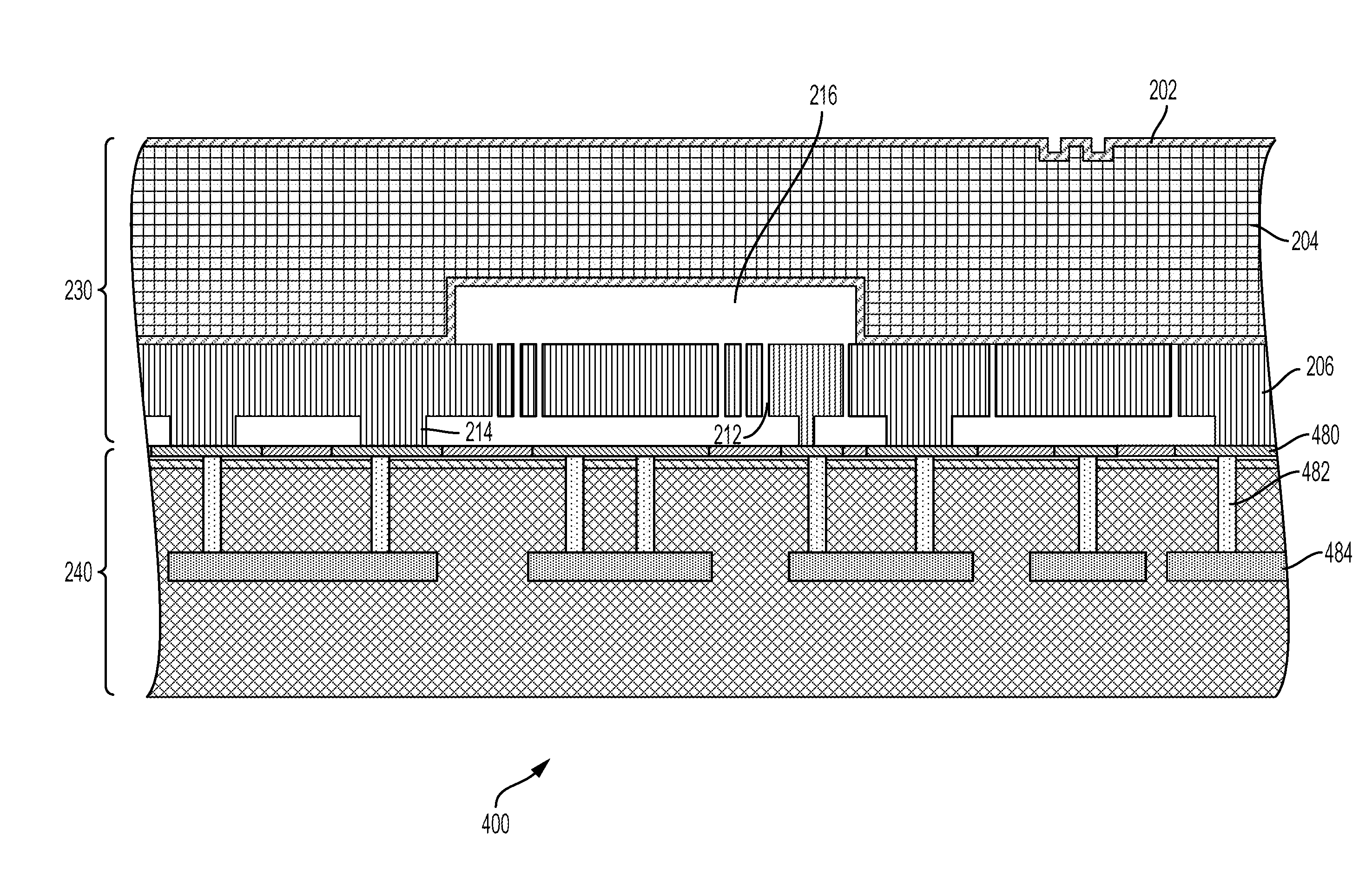
[0031]FIG. 4 illustrates a CMOS-MEMS integrated device 400 using a lower temperature bonding process in accordance with a The CMOS-MEMS integrated device 400 includes the same components 202, 204, 206, 212, 214, and 216 of the MEMS substrate 230 of FIG. 2. However, in FIG. 4, the CMOS substrate includes a layer 480 instead of the new top metal layer of FIG. 2 that is formed as a combination between the top metal layer 210 and the conductive metal layer 218. The layer 480 is coupled to at least one via 482 that interconnects to a buried CMOS metal layer 484. In one embodiment, the layer 480 serves as at least one electrode and at least one bond pad using any of a copper (Cu) and a tungsten (W) metal.

[0032]As in FIG. 2, the lower temperature bonding process of FIG. 4 that utilizes a metal silicide formation enables the removal of the Al-squish process utilized by conventional bonding processes. Without Al-squish, the MEMS Si to M-top sensing electrode gap is just the standoff heights...


PUM

PropertyMeasurementUnit
down forcesaaaaaaaaaa
temperaturesaaaaaaaaaa

Abstract

A method and system for forming a MEMS device are disclosed. In a first aspect, the method comprises providing a conductive material over at least a portion of a top metal layer of a base substrate, patterning the conductive material and the at least a portion of the top metal layer, and bonding the conductive material with a device layer of a MEMS substrate via metal silicide formation. In a second aspect, the MEMS device comprises a MEMS substrate, wherein the MEMS substrate includes a handle layer, a device layer, and an insulating layer in between. The MEMS device further comprises a base substrate, wherein the base substrate includes a top metal layer and a conductive material over at least a portion of the top metal layer, wherein the conductive material is bonded with the device layer via metal silicide formation.

Description

FIELD OF THE INVENTION[0001]The present invention relates to microelectromechanical systems (MEMS) devices, and more particularly, to a complementary metal-oxide-semiconductor (CMOS)-MEMS integration using metal silicide formation.BACKGROUND[0002]Microelectromechanical systems (MEMS) devices are produced using various bonding techniques. Conventional bonding occurs at high temperatures and high down forces which cause thermo-mechanical stress to the MEMS devices thereby rendering the MEMS devices with a parametric shift, or non-functional in the worst case. Therefore, there is a strong need for a solution that overcomes the aforementioned issues. The present invention addresses such a need.SUMMARY OF THE INVENTION[0003]A method and system for forming a MEMS device are disclosed. In a first aspect, the method comprises providing a conductive material over at least a portion of a top metal layer of a base substrate, patterning the conductive material and the at least a portion of the ...

Claims


Application Information

Patent Timeline
Patent Type & Authority Applications(United States)
IPC IPC(8): B81C1/00B81B7/00
CPCB81C1/00238B81B7/0006B81C2203/019B81C2203/036B81B2207/012B81C1/00166B81C2203/0792
Inventor SHIN, JONG ILSMEYS, PETERSHIN, JONGWOO
Owner INVENSENSE
Why Eureka
Try Eureka