Wafer plate and mask arrangement for substrate fabrication

a substrate and mask technology, applied in the field of vacuum processing, can solve the problems of difficult bias application, low throughput, and large trays with complex handling and loading and unloading operations, so as to reduce the risk of accidental movement of substrates, and simplify the handling of substrates

Active Publication Date: 2017-03-02
INTEVAC
View PDF81 Cites 335 Cited by
  • Summary
  • Abstract
  • Description
  • Claims
  • Application Information

AI Technical Summary

Benefits of technology

[0013]Embodiments of the invention provide a system architecture that is modular, in that it enables using different processes and process steps, and versatile, in that it is suitable for fabrication of various devices, including, e.g., solar cells, flat panel displays, touch screens, etc. Moreover, the system can handle different types and sizes of substrates without reconfiguration, but by simply changing the susceptors used.
[0014]The system architecture enables substrate handling, such as loading and unloading in atmospheric environment, separate from the vacuum processing. Additionally, various embodiments enable manual loading and unloading with automation in idle or not present, i.e., the system can be implemented without loading / unloading automation. Inside the vacuum environment the system enables static or pass-by processing of the substrates. In certain embodiments, vacuum isolation is provided between each processing chamber, using actuated valves. Various embodiments provide for electrostatic chucking of the substrates to enable efficient cooling and to prevent accidental movement of the substrates. In other embodiments, mechanical chucking is enabled using, e.g., spring-loaded clips with relief mechanism for loading / unloading of the substrates. Various embodiments also enable biasing of the substrates using, e.g., RF or DC bias power, or floating the substrate.
[0015]Various embodiments enable simplified handling of substrates by having the handling performed on line-array carriers, while processing is performed on a two-dimensional array of n×m substrates, by processing several line-array carriers simultaneously. Other embodiments provide for transport mechanism wherein the substrates are processed in a vertical orientation, but loading and unloading is performed while the substrates are handled horizontally.

Problems solved by technology

Single substrate processing enables high level of control of the process inside the chamber and the resulting film or structure fabricated on the substrate, but results in a relatively low throughput.
While throughput is increased utilizing trays of two-dimensional wafer arrays, the handling and the loading and unloading operations of such large trays becomes complex.
However, since batch system utilize a moving tray with the substrates, it is difficult to apply the bias.
However, loading and unloading of substrate vertically is complex compared to horizontal loading and unloading.
One way to create this exclusion zone is through the use of a mask; however, using masks has many challenges.

Method used


Image

  • Wafer plate and mask arrangement for substrate fabrication
  • Wafer plate and mask arrangement for substrate fabrication
  • Wafer plate and mask arrangement for substrate fabrication

Examples


Embodiment Construction

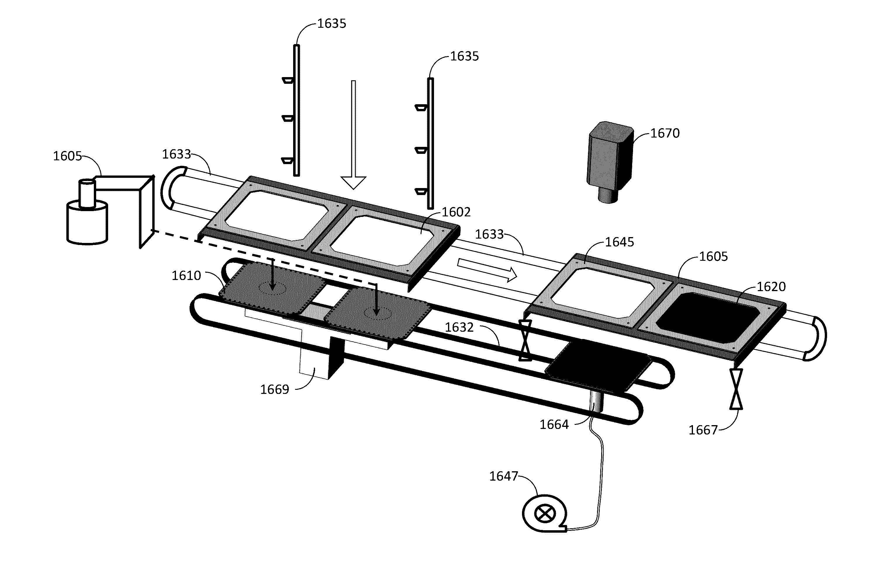
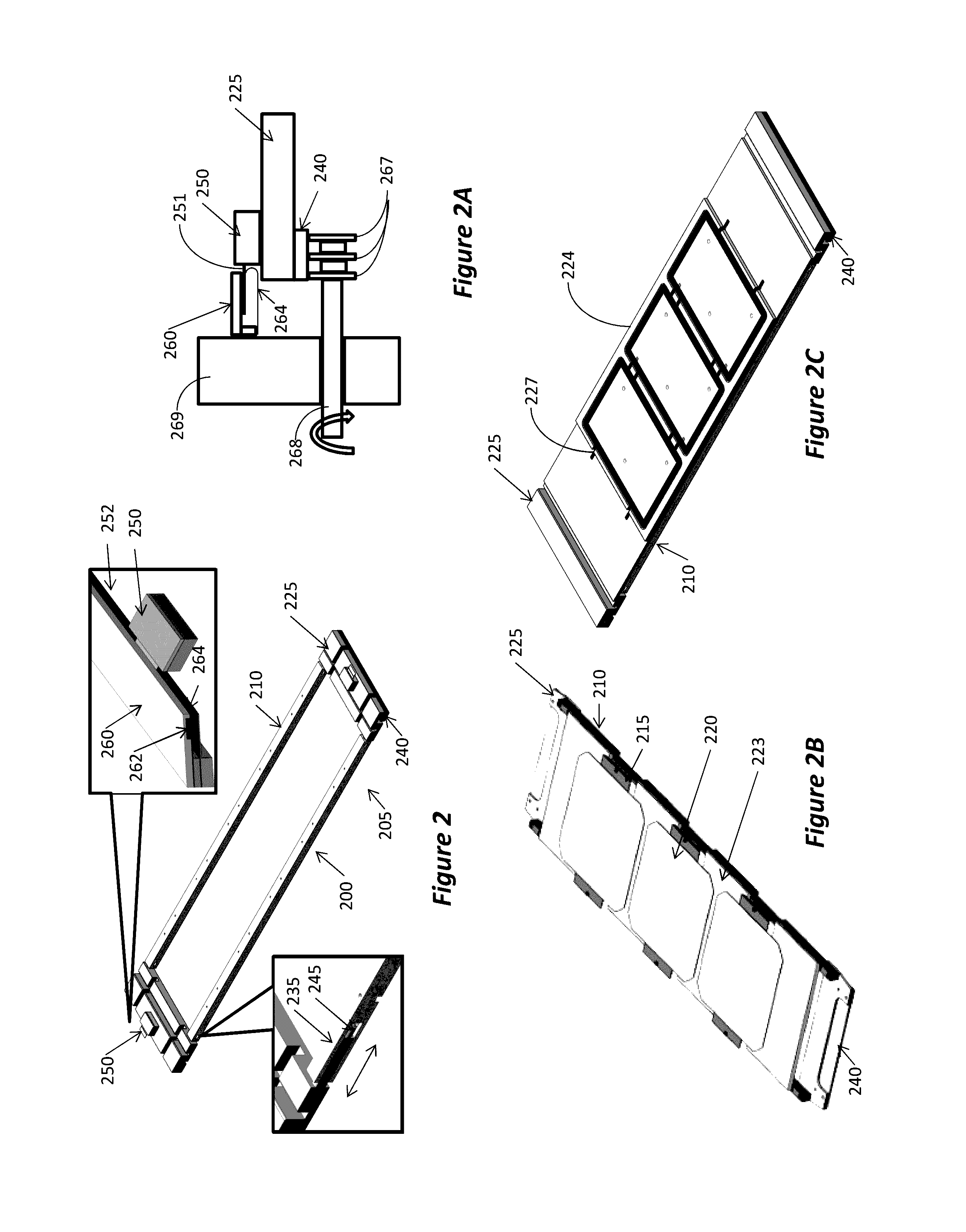
[0043]The following detailed description provides examples that highlight certain features and aspects of the innovative processing system claimed herein. Various disclosed embodiments provide for a system wherein multiple substrates, e.g., semiconductor or glass substrates, are processed simultaneously inside a vacuum processing chamber, such as, e.g., a plasma processing chamber. While glass substrates, such as those used for touchscreens are not generally considered wafers, it should be appreciated that references made to wafers in this disclosure are made for convenience and ease of understanding, but that glass substrates may be substituted for all such references.

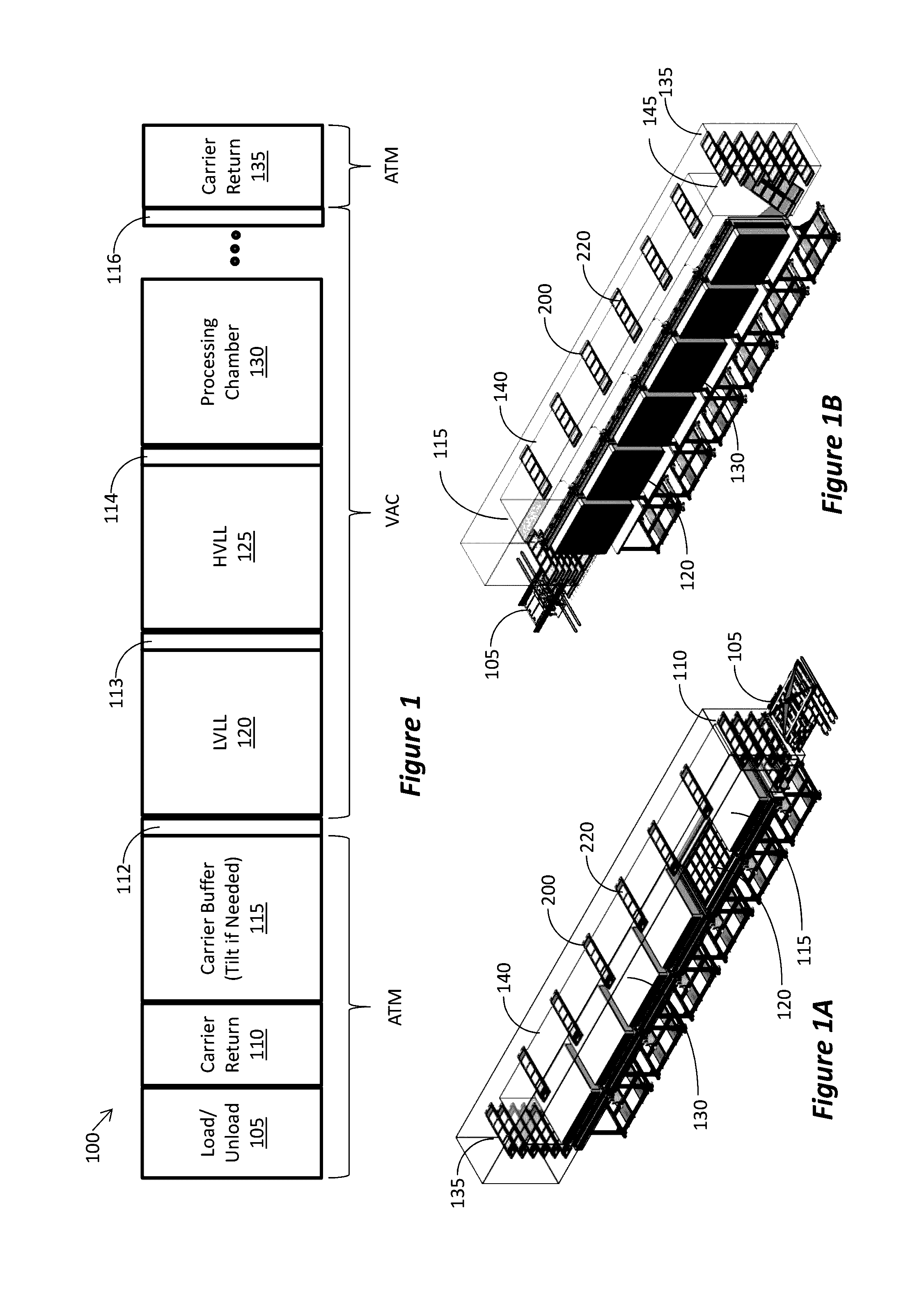
[0044]FIG. 1 is a top-view illustration of an embodiment of a multi-substrate processing system, wherein transport carriers support a line-array of substrates, but processing is performed on a two-dimensional array of substrates. In the system 100 illustrated in FIG. 1, the substrates are loaded and unloaded at load / u...


PUM

PropertyMeasurementUnit
thicknessaaaaaaaaaa
thicknessaaaaaaaaaa
temperatureaaaaaaaaaa

Abstract

A system for processing wafers in a vacuum processing chamber. Carrier comprising a frame having a plurality of openings, each opening configured to accommodate one wafer. A transport mechanism configured to transport the plurality of carriers throughout the system. A plurality of wafer plates configured for supporting wafers. An attachment mechanism for attaching a plurality of wafer plates to each of the carriers, wherein each of the wafer plates is attached to a corresponding position at an underside of a corresponding carrier, such that each of the wafers positioned on one of the wafer carriers is positioned within one of the plurality of opening in the carrier. Mask attached over front side of one of the plurality of opening in the carrier. Alignment stage supports wafer plate under the opening in the carrier. A camera positioned to simultaneously image the mask and the wafer.

Description

RELATED APPLICATIONS[0001]This application claims priority benefit from U.S. Provisional Application No. 62 / 235,898, filed Oct. 1, 2015. This application is also a continuation-in-part of U.S. patent application Ser. No. 13 / 866,856, filed Apr. 19, 2013, and which claims priority benefit from U.S. Provisional Application No. 61 / 639,052, filed Apr. 26, 2012 and U.S. Provisional Application No. 61 / 635,804, filed Apr. 19, 2012. This application is also a continuation-in-part of U.S. patent application Ser. No. 13 / 871,871, filed Apr. 26, 2013, and which claims priority benefit from U.S. Provisional Application No. 61 / 639,052, filed Apr. 26, 2012. The entire disclosures of which are incorporated herein by reference.BACKGROUND[0002]1. Field[0003]This application relates to systems for vacuum processing, such as systems used in the fabrication of solar cells, flat panel displays, touch screens, etc.[0004]2. Related Art[0005]Various systems are known in the art for fabricating semiconductor ...

Claims


Application Information

Patent Timeline
Patent Type & Authority Applications(United States)
IPC IPC(8): H01L21/68H01L21/677H01L21/683
CPCH01L21/682H01L21/681H01L21/67706H01L21/67733H01L21/67736H01L21/6838C23C14/042C23C14/50C23C14/568H01L21/6734H01L21/67346H01L31/18C23C16/042C23C16/4585
Inventor BLUCK, TERRYZANETTO, AARONRUNSTADLER, JR., WILLIAM EUGENEPEDERSON, TERRY
Owner INTEVAC
Why Eureka
Try Eureka