Supercharge Your Innovation With Domain-Expert AI Agents!

On-chip emulation of large resistors for integrating low frequency filters

a low frequency filter and large resistor technology, applied in the field of on-chip emulation of large resistors for integrating low frequency filters, can solve the problems of large die area of resistors, cost prohibitive, and large resistance, and achieve large ir losses, reduce the impact of leakage current, and reduce the effect of cos

Active Publication Date: 2017-03-02
VIDATRONIC
View PDF4 Cites 2 Cited by
  • Summary
  • Abstract
  • Description
  • Claims
  • Application Information

AI Technical Summary

Benefits of technology

The invention describes new ways to put very large resistance on chips while minimizing the impact of leakage currents and switching noise. The techniques use switched capacitors, which don't have any physical resistance that could cause big losses. These techniques also reduce the noise from switching by using a much larger capacitor.

Problems solved by technology

More importantly, these solutions require a very large die area for the resistors.
For most customers, such a solution becomes prohibitive in cost, not to mention the variations in the pole location that can be as high as 100% due to independent variations of the resistor and capacitor over process / temperature and mismatch corners.
Other reasons for trying these methods may be because the process node of choice does not have sheet resistors available for use or requires special extra masks to be ordered, which may be cost prohibitive.
However, these approaches have the following limitations:1. Increased risk of leakage current errors due to parasitic transistors that come inherently with these diodes, especially at high temperatures above 100° C. Even a 10 pA leakage at the node (216) can cause an input offset of 1.63 mV for the case under consideration.
This leakage induced error is a problem even for other applications2. Uncontrollability of the reverse biased off impedance, because this is determined by process recipe (such as doping) to a large extent3. Large variability in the off impedance over process and especially temperature corners, leading to big variations in the pole location being implemented (much more than the case of a physical resistor as explained in the previous paragraph), causing performance issues at the circuit level4. Voltage swing limitations on the input signal to be within a diode drop on both polarities, so as to avoid clipping the input signal appearing at the error amplifier (203) input node (216)5. Variations of the impedance with input signal swing due to the modulating effects on the gate bias, thereby causing non-linear filtering of the input, which is highly undesirable
However, these approaches usually suffer from the following limitations:1. Increased impedance variations due to additional susceptibility to bias variations (VGS) because of common-mode (204) shifts, on top of the process and temperature variations of the transistor parameters.2. Increased risk of leakage current induced voltage drops, as mentioned above, due to the presence of parasitic junctions inherent to the transistor3. Variations of the impedance with input signal swing due to the modulating effects on the gate bias, thereby causing non-linear filtering of the input, which is highly undesirable
However, the down side of this approach is the impact of the amplifier offset and the quiescent current required by the active circuits, which can be big detriments for some applications.

Method used


Image

  • On-chip emulation of large resistors for integrating low frequency filters
  • On-chip emulation of large resistors for integrating low frequency filters
  • On-chip emulation of large resistors for integrating low frequency filters

Examples


Embodiment Construction

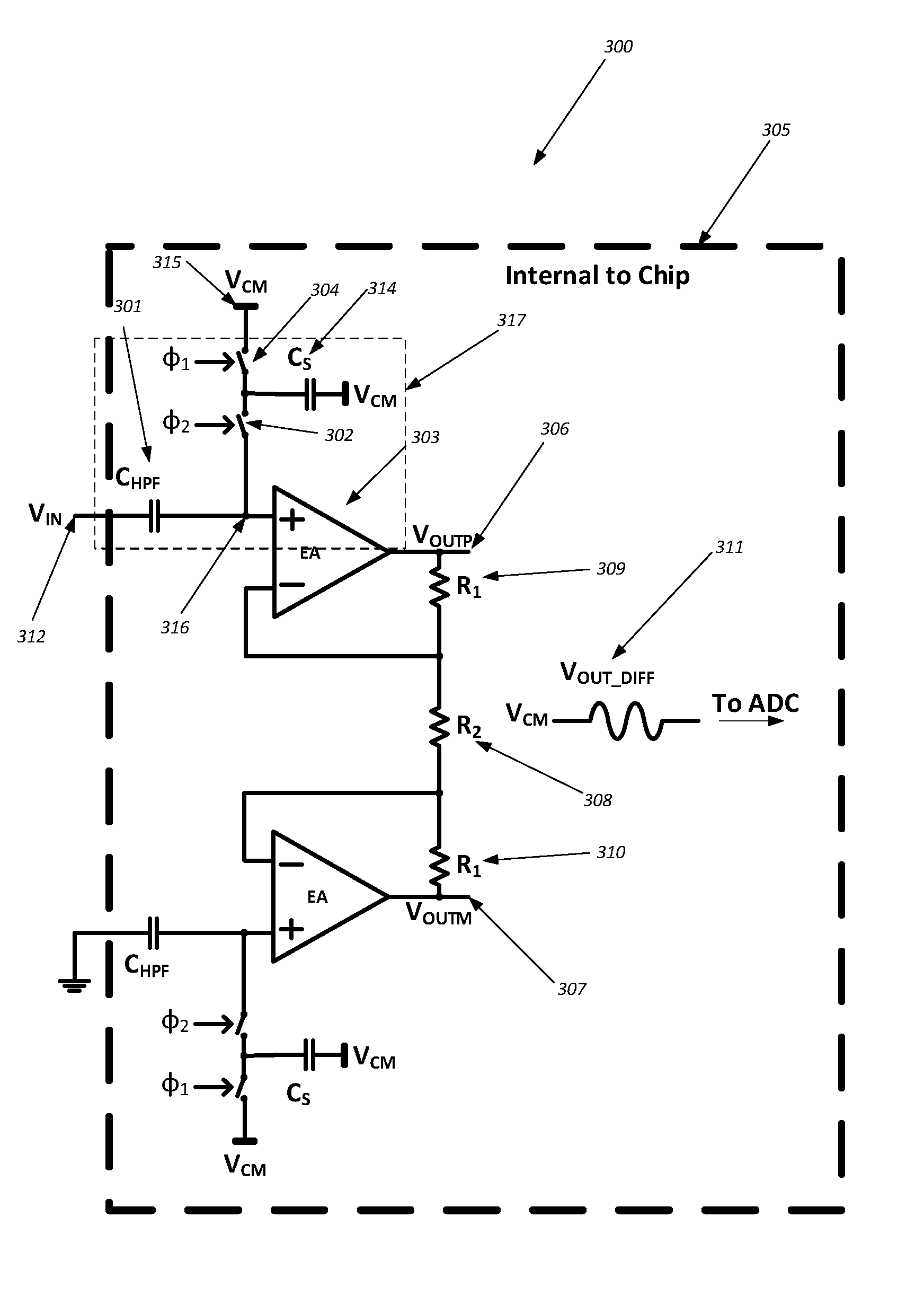
[0034]Aspects of the present disclosure are illustrated in the above-identified drawings and are described below. In the description, like or identical reference numerals are used to identify common or similar elements. The drawings are not necessarily to scale and certain features may be shown exaggerated in scale or in schematic in the interest of clarity and conciseness.

[0035]Embodiments of the invention relate to innovative solutions, which address some or all of the above-mentioned limitations in the prior art and result in a robust solution to the requirement at hand, while also occupying significantly less die area. Embodiments of the invention achieve this by using a switched capacitor scheme to effectively implement a large resistor. Emulating a resistor using a switched capacitor circuit to implement ultra large resistances enables integration of large external input de-coupling capacitors. Embodiments of the invention result in several benefits and make it viable at a sys...


PUM


Abstract

A system for processing of signals with poles that are low in frequency includes a switched capacitor circuit that includes two switches connected to an input and an output of a switching capacitor (Cs), respectively, in an alternating manner at a selected switching frequency (fSW); and a filter capacitor connected between an input and the switched capacitor circuit. The filter capacitor and the switched capacitor circuit together function as a filter, thereby a pole frequency depending on a ratio of capacitance of the switching capacitor (Cs) and the filter capacitor, instead of an RC product.

Description

CROSS REFERENCE TO RELATED APPLICATIONS[0001]This claims the benefits of Provisional Application No. 62 / 211,374, filed on Aug. 28, 2015, the disclosure of which is incorporated by reference in its entirety.BACKGROUND[0002]There are many different markets and applications that require integration of ultra large resistors (>tens of Mega Ohms) in an area-efficient manner, while also achieving as low a variation as possible in the value of the resistance, without having to resort to trimming techniques. In an analog system, this requirement can be anywhere in the chip, either at the boundaries to the external world or deep inside. For simplicity and ease of understanding, an example of a single-ended to differential conversion architecture using a well-known instrumentation amplifier topology is used for illustration.[0003]FIG. 1 shows a schematic block diagram (100) of a single-ended to differential conversion Instrumentation Amplifier architecture (105). As shown in this example, t...

Claims


Application Information

Patent Timeline
Patent Type & Authority Applications(United States)
IPC IPC(8): H03H19/00H03F3/45
CPCH03H19/004H03F2200/261H03F3/45475H03F2203/45528
Inventor RAGHUPATHY, ANAND VEERAVALLI
Owner VIDATRONIC
Features
  • R&D
  • Intellectual Property
  • Life Sciences
  • Materials
  • Tech Scout
  • Unparalleled Data Quality
  • Higher Quality Content
  • 60% Fewer Hallucinations
Learn More