
Substrate-transferred, deep trench isolation silicon-on-insulator (SOI) semiconductor devices formed from bulk semiconductor wafers

Inactive Publication Date: 2017-03-23
QUALCOMM INC
View PDF7 Cites 6 Cited by
  • Summary
  • Abstract
  • Description
  • Claims
  • Application Information

AI Technical Summary

Benefits of technology

This patent describes a method of making semiconductor devices by using a bulk semiconductor wafer that has been separated from other transistors by deep trenches. The bulk body of each transistor is thinned near the back side of the deep trenches to prevent electrical current leakage between transistors. An insulation substrate is then bonded to the bulk semiconductor wafer to form an SOI wafer. This helps to reduce non-linearity and power loss of the transistors and makes the SOI wafer suitable for RF applications.

Problems solved by technology

Also, bulk CMOS devices are not particularly suited for radio frequency (RF) applications in which higher voltages are coupled (e.g., 25V), as bulk CMOS devices encounter device breakdown at higher voltage levels.

Method used


Image

  • Substrate-transferred, deep trench isolation silicon-on-insulator (SOI) semiconductor devices formed from bulk semiconductor wafers
  • Substrate-transferred, deep trench isolation silicon-on-insulator (SOI) semiconductor devices formed from bulk semiconductor wafers
  • Substrate-transferred, deep trench isolation silicon-on-insulator (SOI) semiconductor devices formed from bulk semiconductor wafers

Examples


Embodiment Construction

[0017]With reference now to the drawing figures, several exemplary aspects of the present disclosure are described. The word “exemplary” is used herein to mean “serving as an example, instance, or illustration.” Any aspect described herein as “exemplary” is not necessarily to be construed as preferred or advantageous over other aspects.

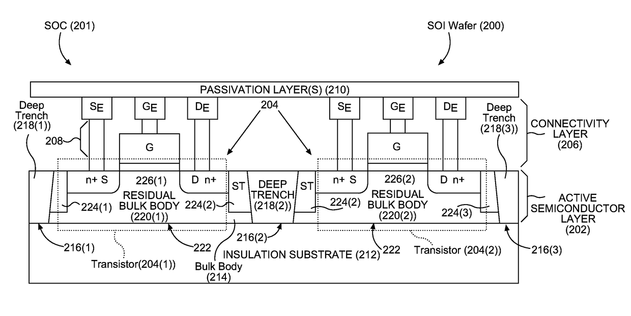
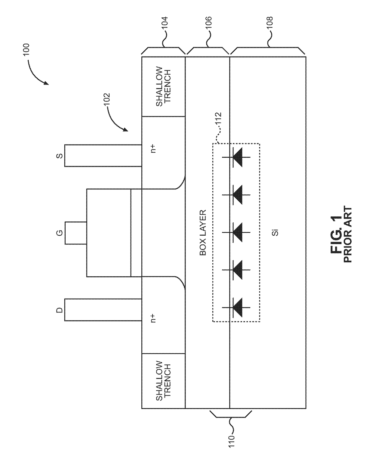
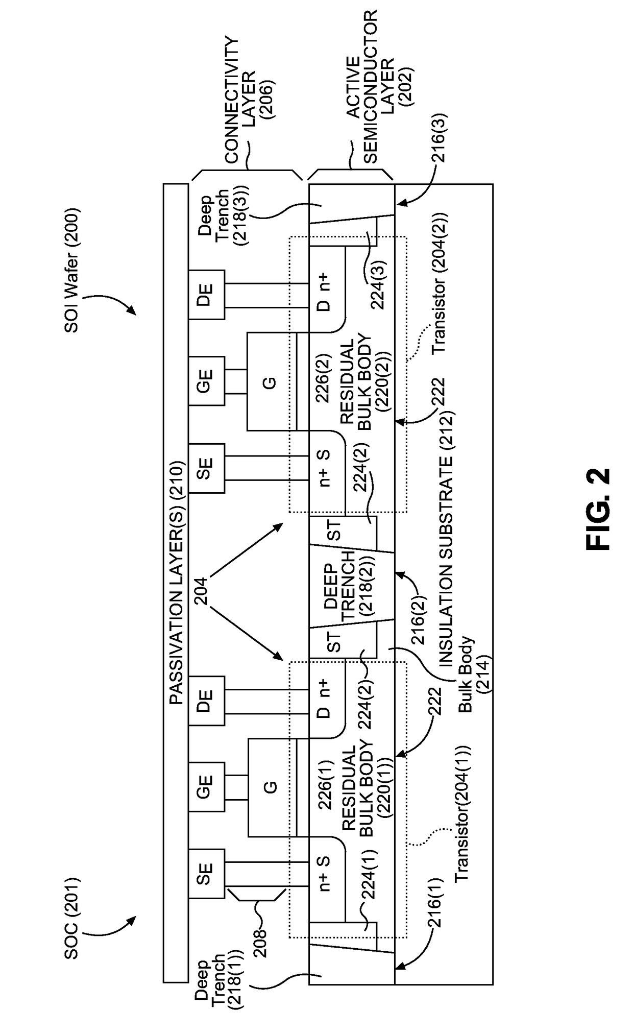
[0018]Aspects disclosed in the detailed description include substrate-transferred, deep trench isolation silicon-on-insulator (SOI) semiconductor devices formed from bulk semiconductor wafers. Related methods and circuits are also disclosed. In this regard, in one aspect, a bulk semiconductor wafer is provided. The bulk semiconductor wafer may be a complementary metal oxide semiconductor (CMOS) device. The bulk semiconductor wafer includes a bulk body layer, also known as a “bulk body.” The bulk body may be a silicon bulk body. One or more transistors are formed in the bulk body of the bulk semiconductor wafer. Deep trenches are formed between the tra...


PUM


Abstract

Substrate-transferred, deep trench isolation silicon-on-insulator (SOI) semiconductor devices formed from bulk semiconductor wafers are disclosed. In this regard, a bulk semiconductor wafer is provided that includes a bulk body, one or more transistors formed in the bulk body, and deep trenches formed between the transistors formed in the bulk body to provide isolation between the transistors. To prevent the bulk body from electrically interconnecting the transistors, the bulk body is thinned near, at, or beyond a back side of the deep trenches formed in the bulk body to form separate bulk bodies for each transistor isolated by the deep trenches. An insulation substrate is bonded to the bulk semiconductor device to form an SOI wafer. In this manner, residual bulk bodies of the transistors in the SOI wafer are isolated between the deep trenches and the insulation substrate to reduce or avoid leakage current between transistors.

Description

BACKGROUND[0001]I. Field of the Disclosure[0002]The technology of the disclosure relates generally to bulk and silicon-on-insulator (SOI) complementary metal oxide semiconductor (CMOS) devices, and particularly to isolation of transistors formed in such devices.[0003]II. Background[0004]Silicon wafers are commonly used for providing semiconductor devices. For example, in a bulk complementary metal oxide semiconductor (CMOS) device, transistors are formed in a bulk silicon body layer. Shallow trench isolation (STI) is employed to provide some isolation between adjacent transistors in the CMOS device. However, the bulk silicon body layer of the transistors in the CMOS device is connected. As a result, the transistors in the CMOS device are not completely isolated. Also, bulk CMOS devices are not particularly suited for radio frequency (RF) applications in which higher voltages are coupled (e.g., 25V), as bulk CMOS devices encounter device breakdown at higher voltage levels.[0005]To pr...

Claims


Application Information

Patent Timeline
IPC IPC(8): H01L27/12H01L21/762
CPCH01L21/76264H01L27/1203H01L21/76256H01L21/76275H01L21/76283H01L21/84H01L21/86H01L29/786
Inventor KIM, DAEIK DANIELYUN, CHANGHAN HOBIELAN, JE-HSIUNG JEFFREYKIM, JONGHAENOWAK, MATTHEW MICHAEL
Owner QUALCOMM INC
Features
  • Generate Ideas
  • Intellectual Property
  • Life Sciences
  • Materials
  • Tech Scout
  • Unparalleled Data Quality
  • Higher Quality Content
  • 60% Fewer Hallucinations
Learn More