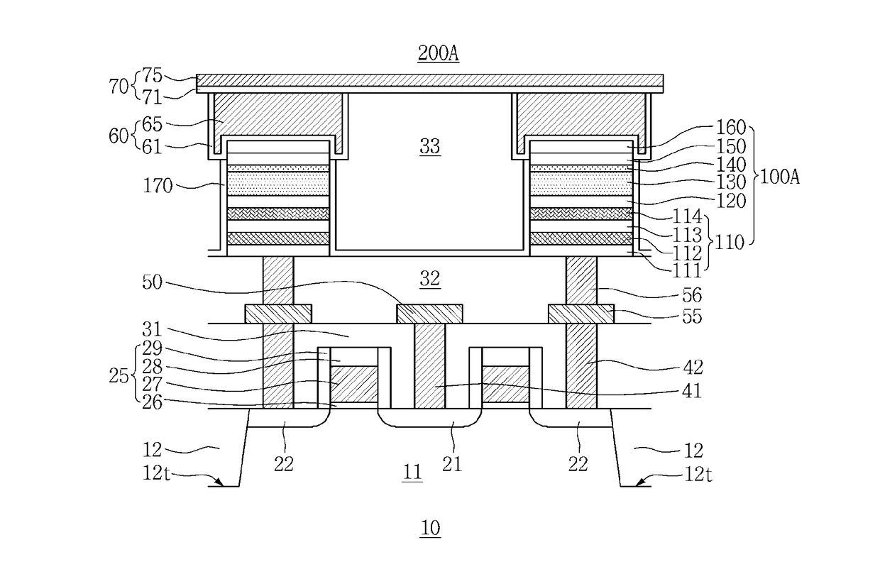
Free layer, magnetoresistive cell, and magnetoresistive random acess memory device having low boron concentration region and high boron concentration region, and methods of fabricating the same

a memory device and magnetoresistive technology, applied in the field of magnetoresistive memory devices, can solve problems such as power consumption

Active Publication Date: 2017-03-23
SAMSUNG ELECTRONICS CO LTD
View PDF1 Cites 12 Cited by
  • Summary
  • Abstract
  • Description
  • Claims
  • Application Information

AI Technical Summary

Problems solved by technology

Present technical challenges associated with the MRAM devices include preserving data for a long time and reducing power consumption.

Method used


Image

  • Free layer, magnetoresistive cell, and magnetoresistive random acess memory device having low boron concentration region and high boron concentration region, and methods of fabricating the same
  • Free layer, magnetoresistive cell, and magnetoresistive random acess memory device having low boron concentration region and high boron concentration region, and methods of fabricating the same
  • Free layer, magnetoresistive cell, and magnetoresistive random acess memory device having low boron concentration region and high boron concentration region, and methods of fabricating the same

Examples


Embodiment Construction

[0027]Various embodiments will now be described more fully with reference to the accompanying drawings in which some embodiments are shown. The subject matter disclosed herein may, however, be embodied in different forms and should not be construed as limited to the embodiments set forth herein. Rather, these embodiments are disclosed so that this disclosure is thorough and complete and fully conveys the subject matter disclosed herein to those skilled in the art. Accordingly, all such modifications are intended to be included within the scope of the claimed subject matter.

[0028]The terminology used herein to describe the disclosed embodiments is not intended to limit the scope of the claimed subject matter. The use herein of a singular form should not preclude the presence of more than one referent. In other words, elements of the disclosed embodiments referred to in the singular form may number one or more, unless the context clearly indicates otherwise. It shall be further unders...


PUM

PropertyMeasurementUnit
concentrationaaaaaaaaaa
magneticaaaaaaaaaa
boride-forming aaaaaaaaaa

Abstract

A method of forming a magnetoresistive memory device includes forming a ferromagnetic layer, forming a tunneling barrier layer on the ferromagnetic layer, forming a first preliminary free magnetic layer (free layer) containing boron (B) on the tunneling barrier layer, forming a first buffer layer on the first preliminary free layer, performing a first annealing process to transition the first preliminary free layer to form a second preliminary free layer and the first buffer layer to form a first boride layer, performing an etching process to remove the first boride layer, forming a second buffer layer on the second preliminary free layer, performing a second annealing process to transition the second preliminary free layer to form a free layer and the second buffer layer to form a second boride layer, and performing an oxidation process to transition the second boride layer to an oxide layer.

Description

CROSS-REFERENCE TO RELATED APPLICATION[0001]This application claims priority under 35 U.S.C. §119 to Korean Patent Application No. 10-2015-0181836 filed on Sep. 17, 2015, the disclosure of which is hereby incorporated by reference in its entirety.BACKGROUND[0002]Embodiments disclosed herein relate to a magnetoresistive memory device, and, more specifically, a free layer, a magnetoresistive cell, and a magnetoresistive memory device including a region having a relatively low concentration of boron (B) and a region having a relatively high concentration of boron (B), and methods of fabricating the same.DESCRIPTION OF RELATED ART[0003]Magnetoresistive random access memory (MRAM) devices, in particular, spin transfer torque MRAM (STT-MRAM) devices, are being spotlighted as a next-generation memory to replace dynamic random access memory (DRAM) devices because MRAM devices are operated at a low current level, enable random access, and have non-volatile characteristics. Present technical ...

Claims


Application Information

Patent Timeline
Patent Type & Authority Applications(United States)
IPC IPC(8): H01L43/12H01L27/22H01L43/10H01L43/02H01L43/08G11C11/16
CPCH01L43/12H01L43/08H01L27/228H01L43/10H01L43/02G11C11/161H10B61/22H10N50/85H10N50/10H10N50/01
Inventor LEE, JOONMYOUNGJANG, YOUNGMANKIM, KIWOONGPARK, YONGSUNG
Owner SAMSUNG ELECTRONICS CO LTD
Why Eureka
Try Eureka