Semiconductor device and power converter

Active Publication Date: 2017-03-30
TOYODA GOSEI CO LTD
View PDF4 Cites 2 Cited by
  • Summary
  • Abstract
  • Description
  • Claims
  • Application Information

AI Technical Summary

Benefits of technology

This patent describes a semiconductor device with a structure that reduces the effects of depletion layers on high carrier concentration areas, which helps to improve the dispersion of electric current and reduce the on resistance while maintaining a high breakdown voltage. The device includes a trench structure and an insulating film that covers the trench, and a high carrier concentration area is provided at a location away from the trench to be located on the substrate side of the trench. This reduces the impact of a depletion layer formed at a p-n junction interface between the first semiconductor layer and the second semiconductor layer on the high carrier concentration area. Overall, this design improves the performance of the semiconductor device.

Problems solved by technology

The inventors of the present application have, however, found that the technique of JP 2009-194065A fails to sufficiently reduce the on resistance since a depletion layer formed at a p-n junction interface between the drift layer (n type) and the channel layer (p type) is extended into the current dispersion layer and thereby interferes with dispersion of the current in the current dispersion layer.
As a result, this reduces the on resistance, while suppressing reduction of the breakdown voltage.

Method used


Image

  • Semiconductor device and power converter
  • Semiconductor device and power converter
  • Semiconductor device and power converter

Examples


first embodiment

A. First Embodiment

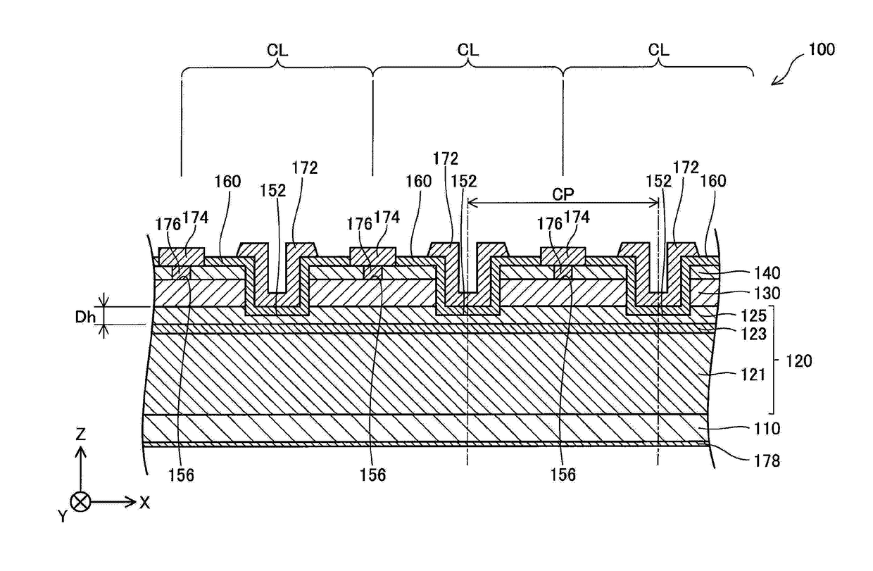
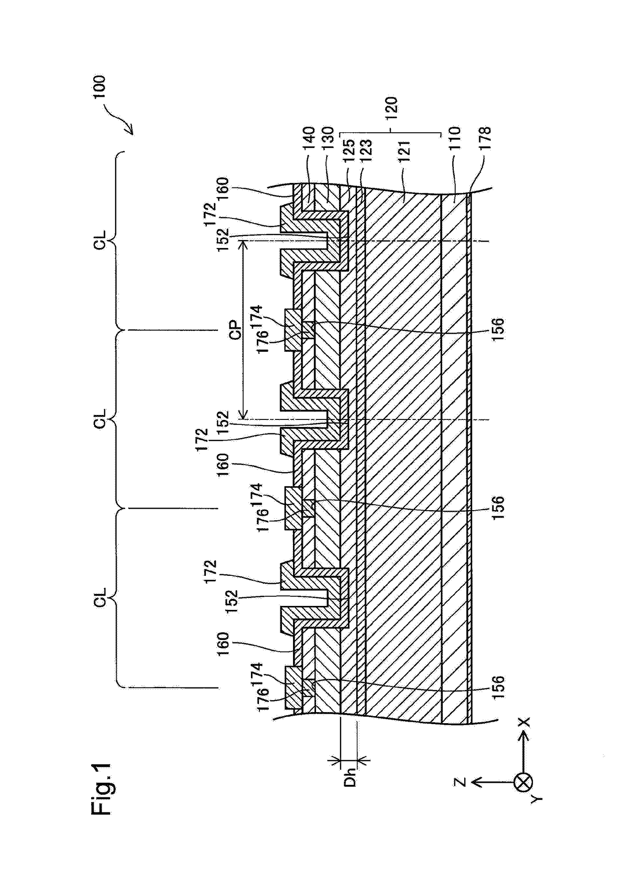
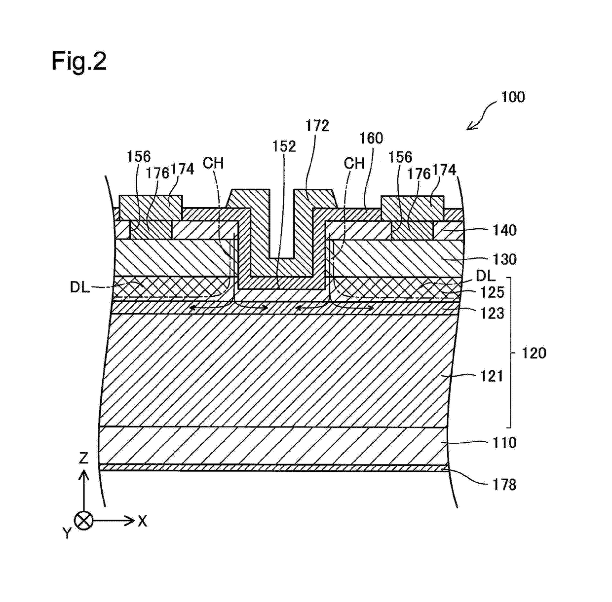
[0026]FIG. 1 is a sectional view schematically illustrating the configuration of a semiconductor device 100. FIG. 2 is an enlarged sectional view illustrating the semiconductor device 100.

[0027]XYZ axes orthogonal to one another are illustrated in FIG. 1. Among the XYZ axes of FIG. 1, the X axis denotes a left-right axis on the sheet surface of FIG. 1. +X-axis direction denotes a rightward direction on the sheet surface, and −X-axis direction denotes a leftward direction on the sheet surface. Among the XYZ axes of FIG. 1, the Y axis denotes a front-back axis on the sheet surface of FIG. 1. +Y-axis direction denotes a backward direction on the sheet surface, and −Y-axis direction denotes a forward direction on the sheet surface. Among the XYZ axes of FIG. 1, the Z axis denotes a top-bottom axis on the sheet surface of FIG. 1. +Z-axis direction denotes an upward direction on the sheet surface, and −Z-axis direction denotes a downward direction on the sheet surface. ...

second embodiment

B. Second Embodiment

[0054]FIG. 3 is an enlarged sectional view illustrating a semiconductor device 100B according to a second embodiment. The XYZ axes are shown in FIG. 3, similarly to FIG. 1.

[0055]The semiconductor device 100B of the second embodiment has a configuration similar to that of the semiconductor device 100 of the first embodiment, except that an n-type semiconductor layer 120B is provided in place of the n-type semiconductor layer 120. The n-type semiconductor layer 120B of the semiconductor device 100B has a configuration similar to that of the n-type semiconductor layer 120 of the first embodiment, except that high carrier concentration areas 123B and low carrier concentration areas 124B are provided in place of the high carrier concentration area 123. The high carrier concentration areas 123B of the n-type semiconductor layer 120B are similar to the high carrier concentration area 123 of the first embodiment, except that the high carrier concentration areas 123B are ...

third embodiment

C. Third Embodiment

[0058]A semiconductor device of a third embodiment has a configuration similar to that of the semiconductor device 100 of the first embodiment, except different specification of a high carrier concentration area 123. The high carrier concentration area 123 of the third embodiment has the carrier concentration of 5.0×1017 cm−3 and the thickness of 0.05 μm but otherwise has a similar configuration to that of the high carrier concentration area 123 of the first embodiment. The configuration of the third embodiment reduces the on resistance while suppressing reduction of the breakdown voltage, like the first embodiment. According to a modification, the high carrier concentration area employed may be, for example, (i) a high carrier concentration area having the carrier concentration of 7.0×1016 cm−3 and the thickness of 0.5 μm or (ii) a high carrier concentration area having the carrier concentration of 1.1×1017 cm−3 and the thickness of 0.5 μm. Employing such a high ...


PUM


Abstract

There is provided a semiconductor device comprising a substrate, a first semiconductor layer, a second semiconductor layer, a third semiconductor layer, a trench and an insulating film arranged to cover a surface of the trench. The first semiconductor layer has a carrier concentration that provides a peak in a thickness direction perpendicular to a plane direction. A high carrier concentration area having a peak of the carrier concentration in the first semiconductor layer is extended in the plane direction at a location away from the trench to be located on the substrate side of the trench. This configuration reduces the on resistance while suppressing reduction of the breakdown voltage in the semiconductor device.

Description

CROSS-REFERENCE TO RELATED APPLICATION[0001]The present application claims priority from Japanese patent applications No. 2015-186506 filed on Sep. 24, 2015 and No. 2016-033752 filed on Feb. 25, 2016, the contents of which are hereby incorporated by reference into this application.BACKGROUND[0002]Technical Field[0003]The invention relates to a semiconductor device and a power converter.[0004]Description of the Related Art[0005]A vertical transistor having a trench gate structure in which a gate electrode is formed in a trench (groove) has been known as a semiconductor device (semiconductor element). JP 2009-194065A discloses a configuration that a current dispersion layer is provided between a drift layer and a channel layer at a depth where a trench is formed in the vertical transistor, for the purpose of reducing the on resistance. This current dispersion layer has similar conductive properties to those of the drift layer but has a higher carrier concentration than the carrier con...

Claims


Application Information

Patent Timeline
IPC IPC(8): H01L29/778H01L29/205H01L29/10H02M1/42H01L29/66H02M7/00H02M7/06H02M1/08H01L29/20H01L29/423
CPCH01L29/7787H01L29/2003H01L29/205H01L29/1045H02M1/42H01L29/66462H02M7/003H02M7/06H02M1/08H01L29/4236H01L29/78H02M1/4225H01L29/7813H01L29/0878H01L29/1095Y02B70/10
Inventor INA, TSUTOMUOKA, TOHRU
Owner TOYODA GOSEI CO LTD
Why Eureka
Try Eureka