Semiconductor light-emitting device

a technology of semiconductor light-emitting devices and semiconductors, which is applied in the direction of semiconductor devices, lasers, semiconductor lasers, etc., can solve the problem that the efficiency of semiconductor devices cannot be readily increased, and achieve the effect of less semiconductor light-emitting device surface defects

Active Publication Date: 2017-05-11
PLAYNITRIDE
View PDF2 Cites 11 Cited by
  • Summary
  • Abstract
  • Description
  • Claims
  • Application Information

AI Technical Summary

Benefits of technology

[0023]Based on the above, the hole injection layer of the semiconductor light-emitting device of an embodiment of the invention is disposed between the P-type semiconductor cladding layer and the light-emitting layer. The hole injection layer includes a first SL structure formed by alternately stacking a plurality of magnesium nitride layers and a plur...

Problems solved by technology

However, these doping methods readily cause defect or dislocation to the semiconductor material lattice, such that the efficacy of the semiconductor device cannot...

Method used


Image

  • Semiconductor light-emitting device
  • Semiconductor light-emitting device
  • Semiconductor light-emitting device

Examples


Embodiment Construction

[0033]Reference will now be made in detail to the present preferred embodiments of the invention, examples of which are illustrated in the accompanying drawings. Wherever possible, the same reference numbers are used in the drawings and the description to refer to the same or like parts.

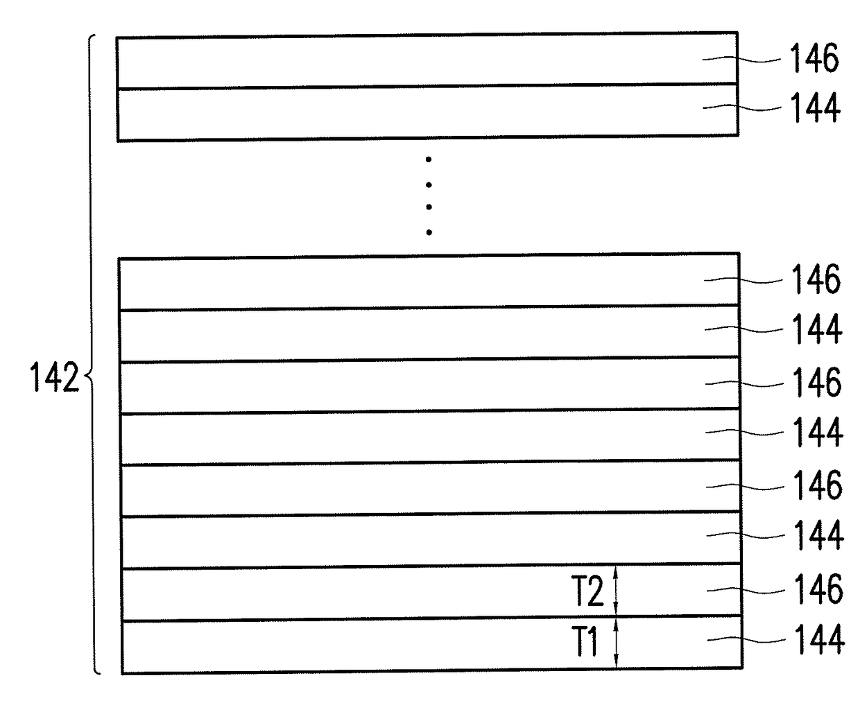
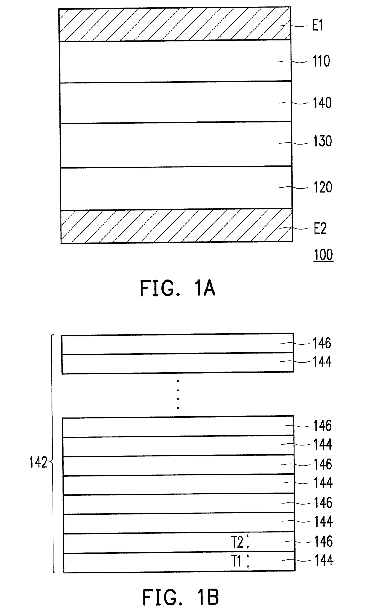
[0034]FIG. 1A is a schematic of a semiconductor light-emitting device of an embodiment of the invention, and FIG. 1B is a schematic of a hole injection layer of the embodiment of FIG. 1A. Please refer to both FIGS. 1A and 1B. It should be mentioned that, to clearly describe each layered structure of the semiconductor light-emitting device, each layered structure of FIG. 1A and FIG. 1B is drawn to proper size and thickness. The invention is not limited to the relationship between the size and the thickness of each layered structure of the semiconductor light-emitting device illustrated in FIG. 1A and FIG. 1B. In the present embodiment, a semiconductor light-emitting device 100 includes a P-type semico...


PUM


Abstract

A semiconductor light-emitting device including a P-type semiconductor cladding layer, an N-type semiconductor layer, a light-emitting layer, and a hole injection layer is provided. The P-type semiconductor cladding layer is doped with magnesium. The light-emitting layer is disposed between the P-type semiconductor cladding layer and the N-type semiconductor layer. The hole injection layer is disposed between the P-type semiconductor cladding layer and the light-emitting layer. The hole injection layer includes a first super lattice structure formed by alternately stacking a plurality of magnesium nitride layers and a plurality of semiconductor material layers. The chemical formula of each of the semiconductor material layers is AlxInyGa1-x-yN, and 0≦x≦1, 0≦y≦1, and 0≦x+y≦1.

Description

CROSS-REFERENCE TO RELATED APPLICATION[0001]This application claims the priority benefit of Taiwan application serial no. 104136951, filed on Nov. 10, 2015. The entirety of the above-mentioned patent application is hereby incorporated by reference herein and made a part of this specification.BACKGROUND OF THE INVENTION[0002]Field of the Invention[0003]The invention relates to a light-emitting device, and more particularly, to a semiconductor light-emitting device.[0004]Description of Related Art[0005]With the rapid development of semiconductor technology, the introduction of semiconductor devices such as light-emitting diodes (LEDs) and laser diodes (LDs) has significantly changed the way we live. LEDs have advantages such as power-saving, small size, short reaction time, and long life, and are currently widely applied in areas of display and illumination. Moreover, LDs have advantages such as high energy efficiency, small size, lightweight, and low price, and are also widely applie...

Claims


Application Information

Patent Timeline
IPC IPC(8): H01L33/06H01L33/32H01L33/58H01S5/20H01S5/343H01S5/30H01S5/34H01L33/02H01L33/14
CPCH01S5/3063H01S5/3086H01S5/3425H01S5/2009H01S5/34333H01L33/025H01L33/32H01L33/58H01L33/145H01L33/06H01S5/3054H01S5/3216H01L33/14H01L33/325
Inventor LAI, YEN-LINWU, JYUN-DE
Owner PLAYNITRIDE
Why Eureka
Try Eureka