Three-Dimensional Semiconductor Device and Manufacturing Method Therefor

a semiconductor memory and three-dimensional technology, applied in the direction of semiconductor memory devices, basic electric elements, electrical appliances, etc., can solve the problems of deteriorating device reliability, difficult to meet the application requirements of some high driving performance, and difficult to perform multi-level cell operation, so as to reduce the off-state leakage current, improve the control characteristics of gate threshold voltage, and prevent the substrate from over-etching

Inactive Publication Date: 2017-06-01
INST OF MICROELECTRONICS CHINESE ACAD OF SCI
View PDF22 Cites 194 Cited by
  • Summary
  • Abstract
  • Description
  • Claims
  • Application Information

AI Technical Summary

Benefits of technology

[0018]In accordance with the three-dimensional semiconductor memory device and manufacturing method of the present invention, the multi-gate MOSFET is formed beneath the stack structure of the memory cell string with vertical channel to serve as the select transistor, this can improve the control characteristics of the gate threshold voltage, reduce the off-state leakage current, prevent the substrate from over-etching, and effectively improve the reliability of the device.

Problems solved by technology

As the size of the memory cells of the two-dimensional (2D) memory devices continues to shrink, signal conflict and interference will significantly increase, so that it is difficult to perform operation of multi-level cell (MLC).
The TCAT device structure has advantages of body-erase (adjusting the control gate can cause the electric potential change of the induced source and drain regions and the floating gate, which can be erased in its entirety) and metal gate (it can be more convenient to adjust the transistor threshold through controlling the work function of the metal material), however, since the select transistor (located above or below the memory transistor cell string) and the storage unit are formed by one cycle of etching and deposition-shaping, it is difficult to accurately adjust the threshold of the select transistor, thereby it is difficult to meet the application requirements of some high driving-performance.
Furthermore, this structure is facing an over-etching problem during the formation process of a vertical channel and a common source, resulting in the deterioration of the device reliability.
However, although the BiCS structure can use the control gate threshold through the stacked placement of the storage array and select transistors respectively, it can only do erasing by gate-induced drain-leaked current (GIRL), unable to do body-erase, which results in low read-write efficiency.

Method used


Image

  • Three-Dimensional Semiconductor Device and Manufacturing Method Therefor
  • Three-Dimensional Semiconductor Device and Manufacturing Method Therefor
  • Three-Dimensional Semiconductor Device and Manufacturing Method Therefor

Examples


first embodiment

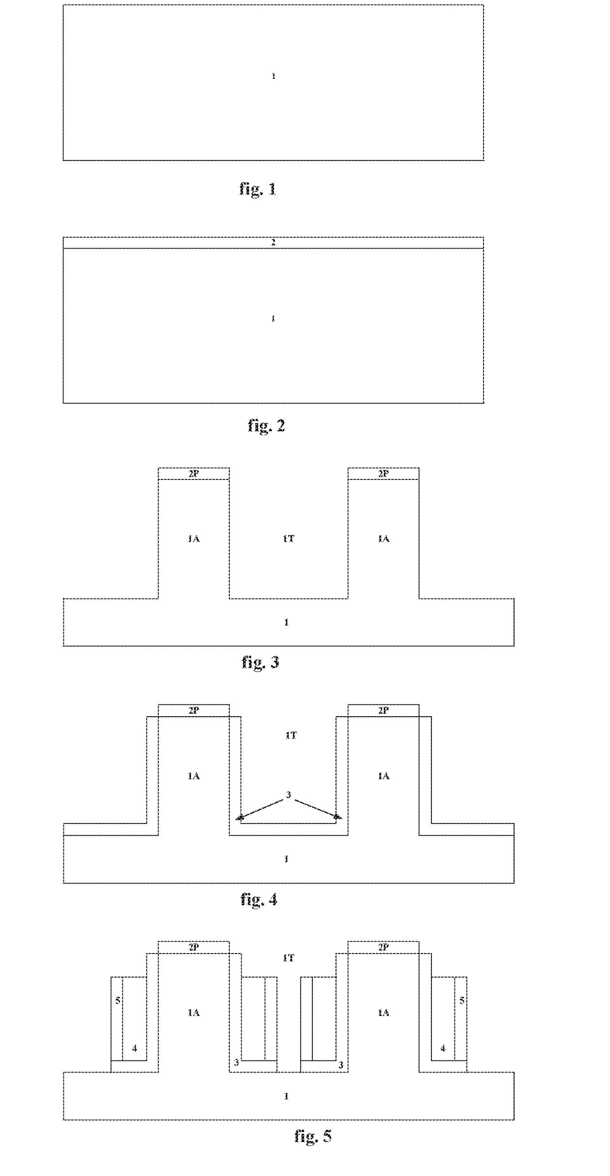
[0023]FIGS. 1 to 16 are cross-sectional views of the various steps of the methods of forming multi-gate select transistor based on the gate-first process and forming memory transistor string thereon in accordance with the present invention.

[0024]As shown in FIG. 1, substrate 1 is provided. The material of substrate 1 may comprise a bulk silicon (bulk Si), bulk germanium (bulk Ge), silicon-on-insulator (SOI), germanium-on-insulator (GeOI), or other compound semiconductor substrate, e.g., SiGe, SiC, GaN, GaAs, InP and the like, and combinations of these substances. For compatibility with the existing IC fabrication process, the substrate 1 is preferably a substrate containing silicon material, e.g., Si, SOI, SiGe, Si:C and the like. Preferably, doping is performed on the substrate 1 to form n- or p-type well region (not shown), to serve as a select transistor well region including a channel region.

[0025]Optionally, as shown in FIG. 2, a hard mask layer 2 is formed on the substrate 1. ...

embodiment 1

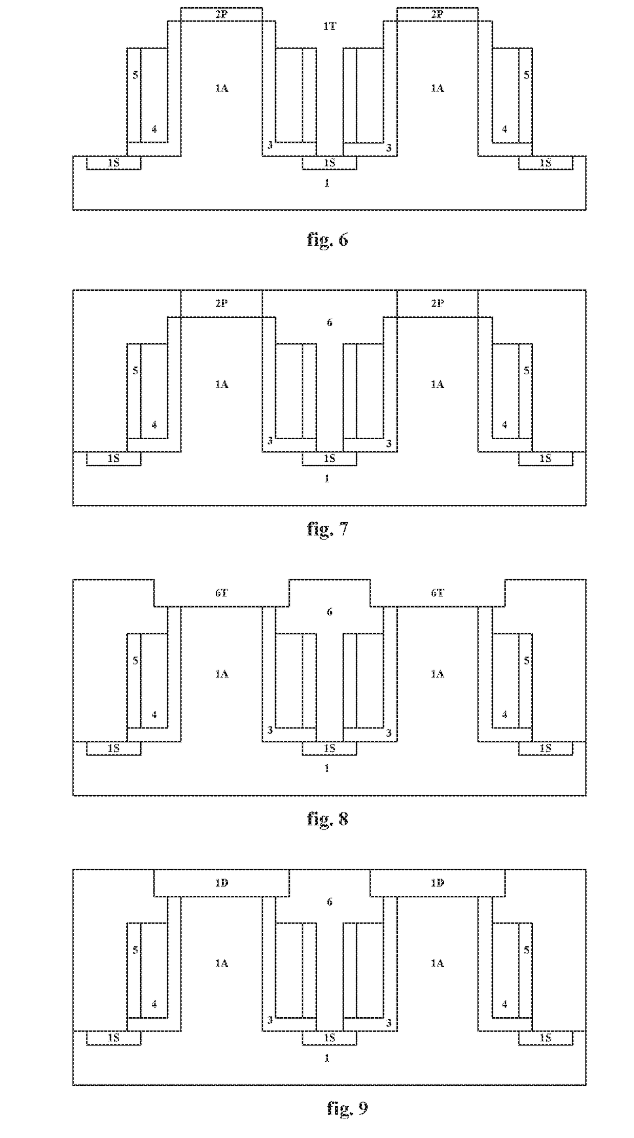
[0043]As shown in FIG. 22, the lateral recesses 2R are filled to form the gate insulating layers 3 and the metal gates 4 of select transistors, as well as the optional gate sidewalls 5. The materials and processes of layers 3 and 4 are as described in Preferably, etch-back process or anisotropic vertical-etching is performed, till the sidewalls of layers 2A are exposed. Similar to FIG. 6, the metal gates 4 are also a dual-gate or multi-gate surrounded structure.

[0044]As shown in FIG. 23, similar to FIG. 9, ILD layer 6 similar to embodiment 1 is deposited over the entire device, and preferably planarized to expose the drain 1D.

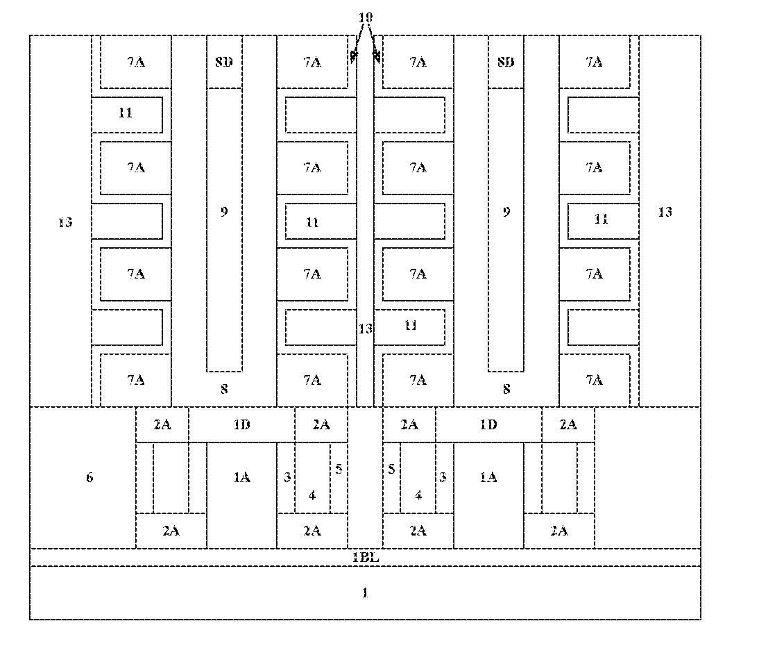
[0045]As shown in FIG. 24, similar to FIG. 10, the stack structure 7 composed of the plurality of first material layers 7A and the second material layers 7B is deposited over the entire device, so as to form a subsequent BiCS structure. The subsequent steps are similar to those shown in FIG. 11 to FIG. 16, no further explanation here.

[0046]As shown in FIG. 25,...


PUM


Abstract

A three-dimensional semiconductor device, comprising a plurality of memory cell transistors and a plurality of select transistors at least partially overlapped in the vertical direction, wherein each select transistor comprises a first drain, an active region and a common source formed in the substrate, distributed along the vertical direction, as well as a metal gate distributed around the active region; wherein each memory cell transistor comprises a channel layer distributed perpendicularly to the substrate surface, a plurality of inter-layer insulating layers and a plurality of gate stack structures alternately stacked along the sidewalls of said channel layer, a second drain located on top of said channel layer; wherein said channel layer and said the first drain are electrically connected. In accordance with the three-dimensional semiconductor memory device and manufacturing method of the present invention, the multi-gate MOSFET is formed beneath the stack structure of the memory cell string including vertical channel to serve as the select transistor, this can improve the control characteristics of the gate threshold voltage, reduce the off-state leakage current, prevent the substrate from over-etching, and effectively improve the reliability of the device.

Description

[0001]This application is a National Phase application of, and claims priority to, PCT Application No. PCT / CN2014 / 081923, filed on Jul. 10, 2014, entitled “3-D Semiconductor Device and Manufacturing Method thereof”, which claimed priority to Chinese Application No. 201410284777.5, filed on Jun. 23, 2014. Both the PCT Application and Chinese Application are incorporated herein by reference in their entireties.TECHNICAL FIELD[0002]The present invention relates to a semiconductor device and manufacturing method thereof, particularly to a three-dimensional semiconductor memory device and manufacturing method thereof.[0003]BACKGROUND TECHNIQUE[0004]In order to improve the density of the memory device, the industry has worked extensively at developing a method for reducing the size of a two-dimensional arrangement of memory cells. As the size of the memory cells of the two-dimensional (2D) memory devices continues to shrink, signal conflict and interference will significantly increase, so...

Claims


Application Information

Patent Timeline
Patent Type & Authority Applications(United States)
IPC IPC(8): H01L27/11582H01L21/28H01L27/1157
CPCH01L27/11582H01L21/28282H01L27/1157H10B41/35H10B41/27H01L29/40117H10B43/27H10B43/35
Inventor HUO, ZONGLIANG
Owner INST OF MICROELECTRONICS CHINESE ACAD OF SCI
Why Eureka
Try Eureka