AI technical title is built by Patsnap AI team. It summarizes the technical point description of the patent document.
a technology of semiconductor devices and semiconductors, applied in semiconductor devices, semiconductor/solid-state device details, electrical apparatus, etc., can solve the problems and achieve the effect of increasing electrical resistance and reducing joint strength
Inactive Publication Date: 2017-06-08
TOYOTA JIDOSHA KK
View PDF3 Cites 6 Cited by
Summary
Abstract
Description
Claims
Application Information
AI Technical Summary
This helps you quickly interpret patents by identifying the three key elements:
Problems solved by technology
Method used
Benefits of technology
Benefits of technology
The patent text discusses a problem where semiconductor elements generate more heat than external components, causing intermetallic compounds to form at the interface between the semiconductor element and the solder joint layer. This can lead to defects that decrease joint strength and increase electrical resistance. The patent provides a solution to suppress the formation of intermetallic compounds and improve the reliability of the semiconductor elements.
Problems solved by technology
If such intermetallic compound is excessively generated, defects such as voids occur, for example, which can cause malfunctions such as a decrease in joint strength, an increase in electrical resistance, and the like.
Method used
Image
Click on the blue label to locate the original text in one second.
Reading with bidirectional positioning of images and text.
Examples
embodiment 1
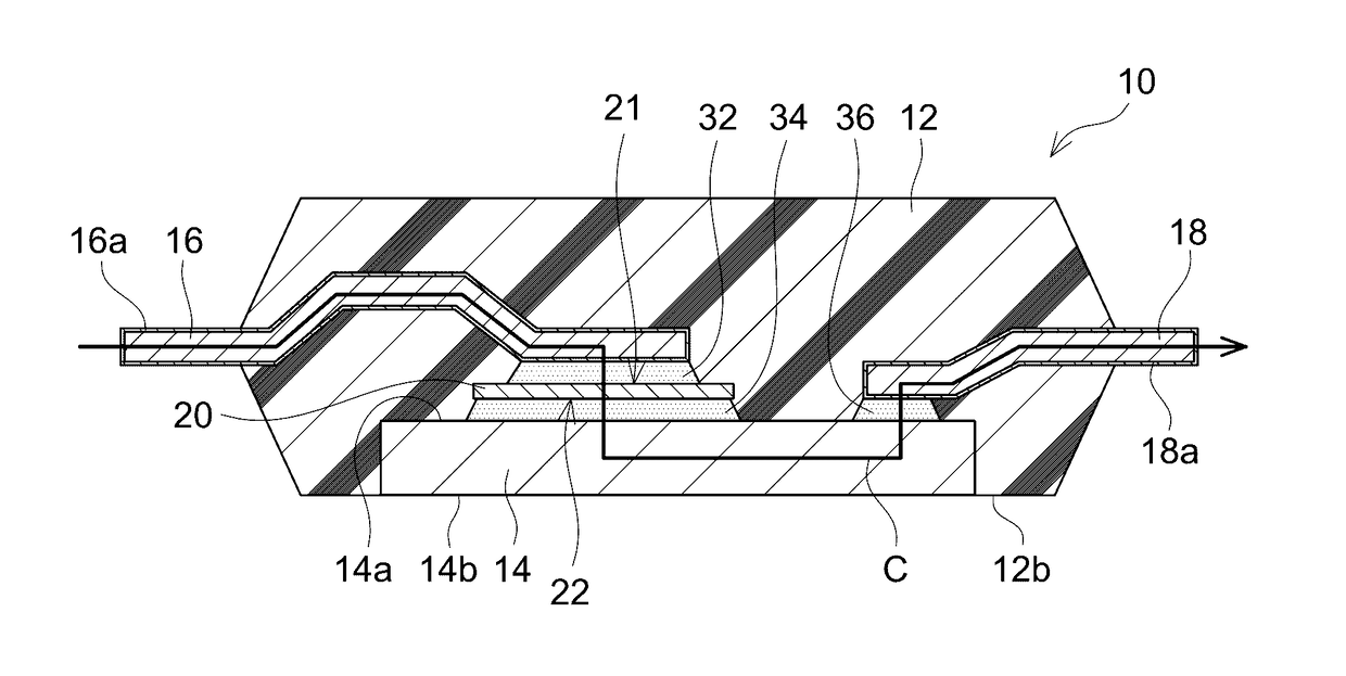
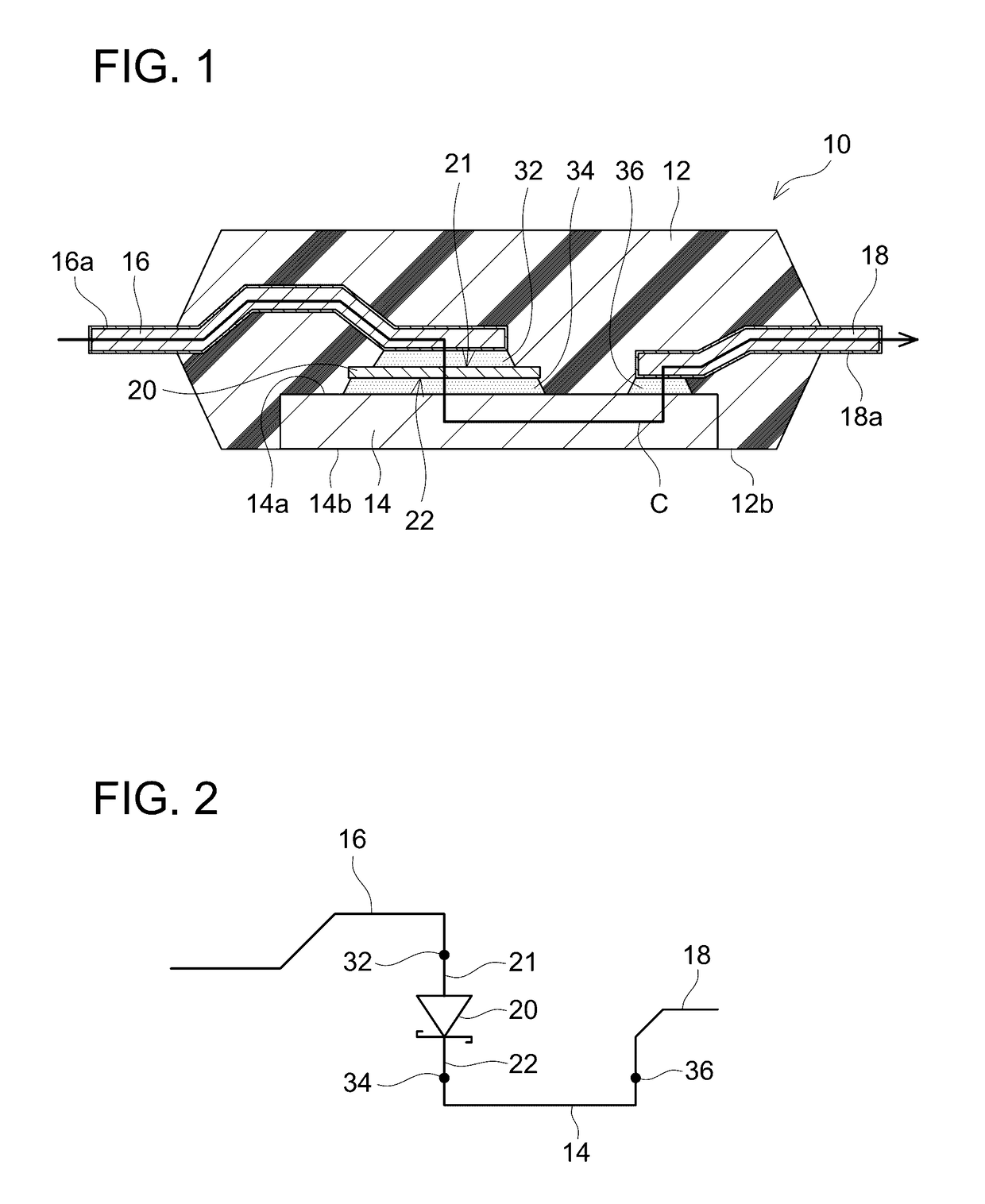
[0026]With reference to the drawings, a semiconductor device 10 in Embodiment 1 will be described. As shown in FIGS, 1 and 2, the semiconductor device 10 includes a semiconductor element 20, and a seal body 12 that seals the semiconductor element 20 therein. The seal body 12 is made of insulating material. The seal body 12 in the present embodiment is the one made of resin material and formed by molding. Notably, the seal body 12 may be made of various sealing materials (or molding materials) such as sealing material for a power semiconductor element can be adopted as appropriate.
[0027]The semiconductor element 20 includes a first electrode 21 and a second electrode 22. The first electrode 21 is located on an upper surface of the semiconductor element 20, and the second electrode 22 is located on a lower surface of the semiconductor element 20. The semiconductor element 20 includes a diode, the first electrode 21 is an anode electrode of the diode, and the second electrode 22 is a c...
embodiment 2
[0041]A semiconductor device 50 in Embodiment 2 will be described. As shown in FIGS. 8 to 12, the semiconductor device 50 includes a plurality of semiconductor elements 70, 80, 90, and 100, and a seal body 52 that seals the plurality of semiconductor elements 70, 80, 90, and 100 therein. Moreover, the semiconductor device 50 includes a plurality of heat sinks 62, 64, 66, and 68, and a plurality of spacers 74, 84, 94, and 104. The plurality of heat sinks 62, 64, 66, and 68 include a first heat sink 62, a second heat sink 64, a third heat sink 66, and a fourth heat sink 68. Each of the heat sinks 62, 64, 66, and 68 and each of the spacers 74, 84, 94, and 104 are electrically conductive members, and are formed of copper in the present embodiment. As mentioned below, each of the heat sinks 62, 64, 66, and 68 and each of the spacers 74, 84, 94, and 104 are electrically connected to one or the plurality of semiconductor elements 70, 80, 90, and 100, and configure an electrically conductiv...
PUM
Abstract
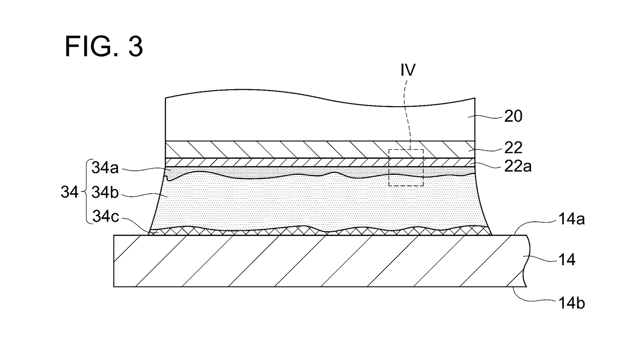
A semiconductor device includes a semiconductor element and an electrically conductive member. The semiconductor element is configured to allow an electric current to flow from a first electrode to a second electrode and prevent an electric current flowing from the second electrode to the first electrode. The electrically conductive member is joined with the second electrode via a solder joint layer. Surface of the second electrode in contact with the solder joint layer mainly comprises nickel, and surface of the electrically conductive member in contact with the solder joint layer mainly comprises copper. The solder joint layer comprises first and second compound layers. The first compound layer is located at an interface with, the second electrode and comprises nickel-tin based intermetallic compound. The second compound layer is located at an interface with the electrically conductive member and comprises copper-tin based intermetallic compound.
Description
CROSS-REFERENCE TO RELATED APPLICATION[0001]This application claims priority to Japanese Patent Application No. 2015-237931 filed on Dec. 4, 2015, the entire contents of which are hereby incorporated by reference into the present application.TECHNICAL FIELD[0002]The disclosure herewith relates to a semiconductor device.DESCRIPTION OF RELATED ART[0003]Japanese Patent Application Publication No. 2002-270736 (JP 2002-270736 A) discloses a semiconductor device. This semiconductor device includes a semiconductor element, and an electrically conductive member joined with an electrode of the semiconductor element. The electrode of the semiconductor element and the electrically conductive member are joined by soldering, and a solder joint layer is formed therebetween. Generally, in a case of joining two members with solder, a nickel film is commonly formed on a surface of each of the members, for the purpose of improving solderability, for example. Notably, the solder mentioned in the prese...
Claims
Application Information
Patent Timeline
Application Date:The date an application was filed.
Publication Date:The date a patent or application was officially published.
First Publication Date:The earliest publication date of a patent with the same application number.
Issue Date:Publication date of the patent grant document.
PCT Entry Date:The Entry date of PCT National Phase.
Estimated Expiry Date:The statutory expiry date of a patent right according to the Patent Law, and it is the longest term of protection that the patent right can achieve without the termination of the patent right due to other reasons(Term extension factor has been taken into account ).
Invalid Date:Actual expiry date is based on effective date or publication date of legal transaction data of invalid patent.
Patent Type & AuthorityApplications(United States)

