NANOWIRE METAL-OXIDE SEMICONDUCTOR (MOS) FIELD-EFFECT TRANSISTORS (FETs) (MOSFETs) EMPLOYING A NANOWIRE CHANNEL STRUCTURE HAVING ROUNDED NANOWIRE STRUCTURES

a metal-oxide semiconductor and nanowire channel technology, applied in the field of nanowire channels, to achieve the effect of reducing the distance between adjacent nanowire channel structures, reducing leakage current, and small channel length

Inactive Publication Date: 2017-06-15
QUALCOMM INC
View PDF0 Cites 24 Cited by
  • Summary
  • Abstract
  • Description
  • Claims
  • Application Information

AI Technical Summary

Benefits of technology

[0010]Aspects of the present disclosure involve nanowire metal-oxide semiconductor (MOS) Field-Effect Transistors (FETs) (MOSFETs) employing a nanowire channel structure having rounded nanowire structures. The use of a nanowire channel structure provides for an effective smaller channel length for a given drive strength with strong gate control of the channel to reduce leakage current. Reducing the distance between adjacent nanowire channel structures in a nanowire MOSFET reduces parasitic capacitances, thereby reducing delay of the nanowire MOSFET and / or increasing frequency performance. However, there is a minimum distance required between adjacent nanowire channel structures due to fabrication limitations to allow gate material to be disposed to surround the nanowire structures to provide sufficient gate control of the channel. In this regard, to allow the separation distance between adjacent nanowire structures to be reduced to further reduce parasitic capacitance while providing sufficient gate control of the channel, the nanowire channel structure employs rounded nanowire structures. For example, the rounded nanowire structures provide for a decreased height moving from a center area of the rounded nanowire structures to end portions of the rounded nanowire structures. Gate material is disposed around rounded end portions of the rounded nanowire structures to extend into at least a portion of the separation area between the adjacent rounded nanowire structures. The gate material may not completely surround the adjacent rounded nanowire structures. The gate material extends in the separation area between the adjacent nanowire rounded structures sufficient to create a fringing field to the channel where gate material is not adjacently disposed, to still provide strong gate control of the channel even though the gate material does not completely surround the rounded nanowire structures.
[0011]Note that the rounded nanowire structures provided in nanowire channel structures in MOSFETs disclosed herein can be provided in any form of nanowire. For example, the rounded nanowire channel structures can be provided as rounded nanowires, nanoslabs, and / or nanosheets. As another example, the rounded nanowire channel structures can also be provided in the form of rounded nanowire structures that have substantially the same width axis in an orthogonal axis in a cross-section of the rounded nanowire channel structures. As another example, the rounded nanowire channel structures can also be provided in the form of rounded nanoslabs that are elongated in an axis from an orthogonal axis in a cross-section of the rounded nanoslabs to increase the width of the nanowire channel structure to further increase drive strength and further reduce parasitic capacitance for further enhanced frequency performance. As another example, the rounded nanowire channel structures can also be provided in the form of rounded nanosheets that are substantially elongated in an axis from an orthogonal axis in a cross-section of the rounded nanosheets to increase the width of the rounded nanowire channel structures to further increase drive strength and further reduce parasitic capacitance for further enhanced frequency performance.

Problems solved by technology

However, there is a minimum distance required between adjacent nanowire channel structures due to fabrication limitations to allow gate material to be disposed to surround the nanowire structures to provide sufficient gate control of the channel.

Method used


Image

  • NANOWIRE METAL-OXIDE SEMICONDUCTOR (MOS) FIELD-EFFECT TRANSISTORS (FETs) (MOSFETs) EMPLOYING A NANOWIRE CHANNEL STRUCTURE HAVING ROUNDED NANOWIRE STRUCTURES
  • NANOWIRE METAL-OXIDE SEMICONDUCTOR (MOS) FIELD-EFFECT TRANSISTORS (FETs) (MOSFETs) EMPLOYING A NANOWIRE CHANNEL STRUCTURE HAVING ROUNDED NANOWIRE STRUCTURES
  • NANOWIRE METAL-OXIDE SEMICONDUCTOR (MOS) FIELD-EFFECT TRANSISTORS (FETs) (MOSFETs) EMPLOYING A NANOWIRE CHANNEL STRUCTURE HAVING ROUNDED NANOWIRE STRUCTURES

Examples


Embodiment Construction

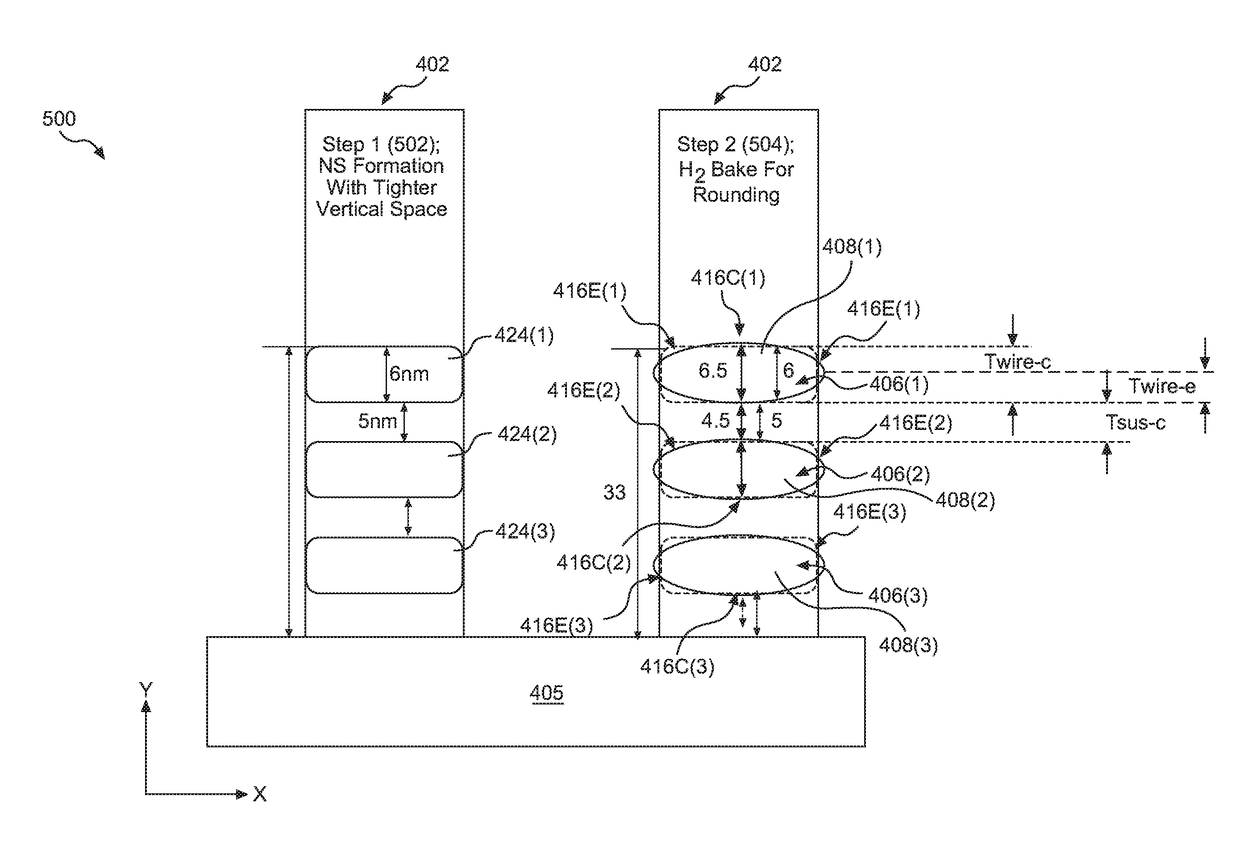
[0033]With reference now to the drawing figures, several exemplary aspects of the present disclosure are described. The word “exemplary” is used herein to mean “serving as an example, instance, or illustration.” Any aspect described herein as “exemplary” is not necessarily to be construed as preferred or advantageous over other aspects.

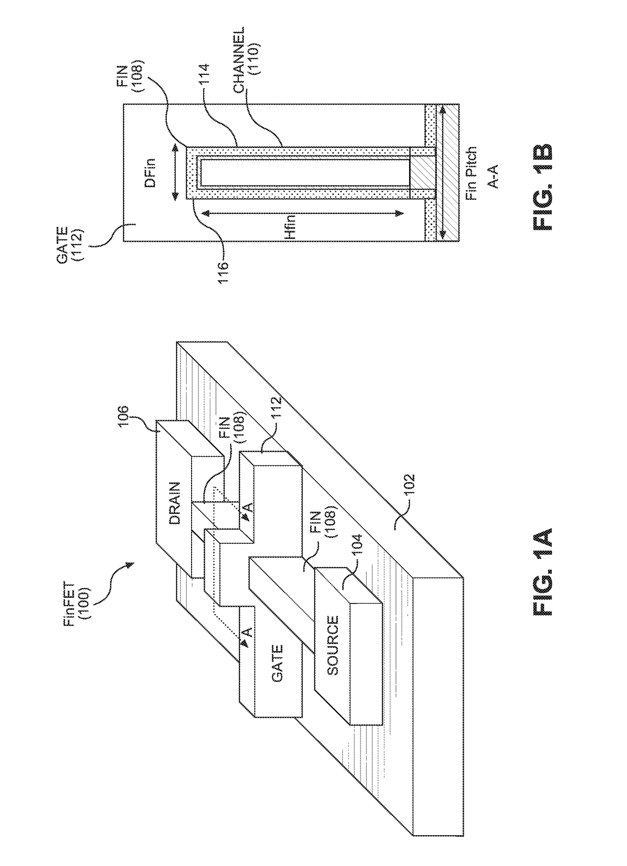
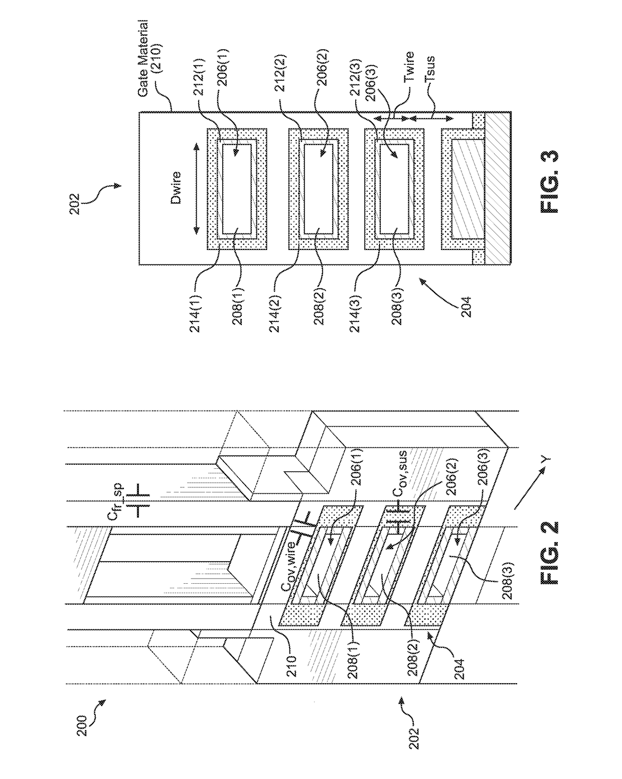
[0034]Aspects of the present disclosure involve nanowire metal-oxide semiconductor (MOS) Field-Effect Transistors (FETs) (MOSFETs) employing a nanowire channel structure having rounded nanowire structures. The use of a nanowire channel structure provides for an effective smaller channel length for a given drive strength with strong gate control of the channel to reduce leakage current. Reducing the distance between adjacent nanowire channel structures in a nanowire MOSFET reduces parasitic capacitances, thereby reducing delay of the nanowire MOSFET and / or increasing frequency performance. However, there is a minimum distance required between adjacent ...


PUM

PropertyMeasurementUnit
sizesaaaaaaaaaa
sizesaaaaaaaaaa
sizesaaaaaaaaaa

Abstract

Nanowire metal-oxide semiconductor (MOS) Field-Effect Transistors (FETs) (MOSFETs) employing a nanowire channel structure having rounded nanowire structures is disclosed. To reduce the distance between adjacent nanowire structures to reduce parasitic capacitance while providing sufficient gate control of the channel, the nanowire channel structure employs rounded nanowire structures. For example, the rounded nanowire structures provide for a decreased height from a center area of the rounded nanowire structures to end areas of the rounded nanowire structures. Gate material is disposed around rounded ends of the rounded nanowire structures to extend into a portion of separation areas between adjacent nanowire structures. The gate material extends in the separation areas between adjacent nanowire structures sufficient to create a fringing field to the channel where gate material is not adjacently disposed, to provide strong gate control of the channel even though gate material does not completely surround the rounded nanowire structures.

Description

PRIORITY APPLICATIONS[0001]This patent application claims priority under 35 U.S.C. §119(e) to U.S. Provisional Patent Application Ser. No. 62 / 267,449 filed on Dec. 15, 2015 and entitled “NANOWIRE METAL-OXIDE SEMICONDUCTOR (MOS) FIELD-EFFECT TRANSISTORS (FETs) (MOSFETs) EMPLOYING A NANOWIRE CHANNEL STRUCTURE HAVING ROUNDED NANOWIRE STRUCTURES,” which is incorporated herein by reference in its entirety.[0002]This patent application also claims priority under 35 U.S.C. §119(e) to U.S. Provisional Patent Application Ser. No. 62 / 294,361 filed on Feb. 12, 2016 and entitled “NANOWIRE METAL-OXIDE SEMICONDUCTOR (MOS) FIELD-EFFECT TRANSISTORS (FETs) (MOSFETs) EMPLOYING A NANOWIRE CHANNEL STRUCTURE HAVING ROUNDED NANOWIRE STRUCTURES,” which is incorporated herein by reference in its entirety.BACKGROUND[0003]I. Field of the Disclosure[0004]The technology of the disclosure relates generally to metal-oxide semiconductor (MOS) Field-Effect Transistors (FETs) (MOSFETs), and more particularly to the...

Claims


Application Information

Patent Timeline
Patent Type & Authority Applications(United States)
IPC IPC(8): H01L29/06H01L21/324H01L27/088H01L21/02H01L29/78H01L29/66
CPCH01L29/0673H01L29/785H01L29/66795H01L21/324H01L27/0886H01L21/02603H01L29/0649H01L29/401H01L29/42364H01L29/42392H01L29/66439H01L29/775H01L29/7853H01L29/7854H01L29/78696
Inventor SONG, STANLEY SEUNGCHULFENG, PEIJIERIM, KERNXU, JEFFREY JUNHAOYEAP, CHOH FEI
Owner QUALCOMM INC
Why Eureka
Try Eureka