Drain extension region for tunnel fet

a tunnel fet and drain extension technology, applied in the field ofsemiconductor devices, can solve the problems of difficult optimization of ss and on-current, limited ss to 60 mv/decade, and low ss value of transistors operating under btbt, and achieve good current characteristics and easy manufacturing

Active Publication Date: 2017-06-15
INTERUNIVERSITAIR MICRO ELECTRONICS CENT (IMEC VZW) +1
View PDF2 Cites 4 Cited by
  • Summary
  • Abstract
  • Description
  • Claims
  • Application Information

AI Technical Summary

Benefits of technology

[0005]It is an object of the embodiments to provide a transistor easy to manufacture, fast and with good current characteristics, such as a suppressed OFF current.

Problems solved by technology

In traditional Metal-Oxide-Semiconductor Field-Effect Transistors (MOSFETs) at room temperature, this SS is limited to 60 mV / decade at room temperature due to the thermal energy of the carriers and the capacitance of the transistors.
Transistors operating under BTBT can reach lower SS values, but often at the cost of a lower ON-current.
For example, IV materials as well as mixtures of III-V materials have been implemented in TFETs, but the optimization of both SS and ON-currents is challenging.
Unfortunately, the gate-drain underlap and the reduced drain doping concentration limit the maximum current through the TFET.

Method used


Image

  • Drain extension region for tunnel fet
  • Drain extension region for tunnel fet
  • Drain extension region for tunnel fet

Examples


Embodiment Construction

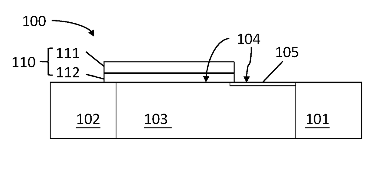
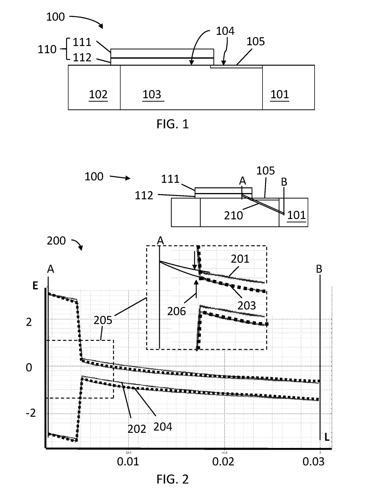
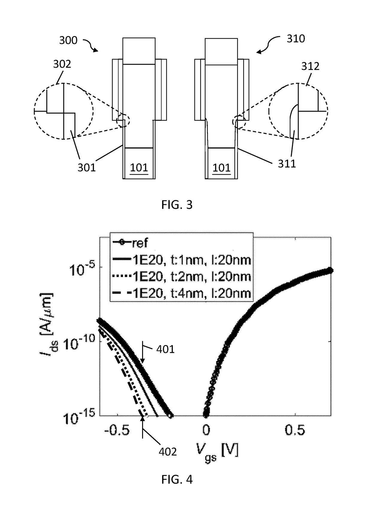
[0030]The present disclosure will be described with respect to particular embodiments and with reference to certain drawings but the disclosure is not limited thereto but only by the claims. The drawings described are only schematic and are non-limiting. In the drawings, the size of some of the elements may be exaggerated and not drawn to scale for illustrative purposes. The dimensions and the relative dimensions do not correspond to actual reductions to practice of the disclosure.

[0031]The terms first, second and the like in the description and in the claims, are used for distinguishing between similar elements and not necessarily for describing a sequence, either temporally, spatially, in ranking or in any other manner. It is to be understood that the terms so used are interchangeable under appropriate circumstances and that the embodiments of the disclosure described herein are capable of operation in other sequences than described or illustrated herein.

[0032]Moreover, the terms ...


PUM


Abstract

A Tunnel Field-Effect Transistor comprising a source-channel-drain structure, the source-channel-drain structure comprising a source region doped with a dopant element having a first dopant type and a first doping concentration; a drain region doped with a dopant element having a second dopant type opposite compared to the first dopant type, and a second doping concentration, a channel region situated between the source region and the drain region and having an intrinsic doping concentration, or lowly doped concentration being lower than the doping concentration of the source and drain regions, a gate stack comprising a gate electrode on a gate dielectric layer, the gate stack covering at least part of the channel region and extending at the source side up to at least an interface between the source region and the channel region, a drain extension region in the channel region or on top thereof, the drain extension region being formed from a material suitable for creating, and having a length / thickness ratio such that, in use, it creates a charged layer, in the OFF-state of the TFET, with a charge opposite to the charge of the majority carriers in the drain region.

Description

INCORPORATION BY REFERENCE TO RELATED APPLICATION[0001]Any and all priority claims identified in the Application Data Sheet, or any correction thereto, are hereby incorporated by reference under 37 CFR 1.57. This application claims the benefit of European Application No. EP 15201734.9, filed on Dec. 12, 2015. The aforementioned application is incorporated by reference herein in its entirety, and is hereby expressly made a part of this specification.FIELD OF THE DISCLOSURE[0002]Field Effect Transistors (FETs) based on band-to-band tunneling are provided, for use in the field of semiconductor devices.BACKGROUND OF THE DISCLOSURE[0003]In transistor technology, several parameters and combinations thereof play an important role in determining the applicability range and transistor speed, which have to be combined with size and semiconductor integration requirements of micro- and nanoelectronics. For example, the current that the transistor allows to flow when the transistor is in on-stat...

Claims


Application Information

Patent Timeline
Patent Type & Authority Applications(United States)
IPC IPC(8): H01L29/78H01L29/417H01L29/423H01L29/36
CPCH01L29/7835H01L29/36H01L29/7831H01L29/42356H01L29/41775H01L29/4234H01L29/42364H01L29/7391H01L29/0834
Inventor VERHULST, ANNEVERRECK, DEVINALIAN, ALIREZA
Owner INTERUNIVERSITAIR MICRO ELECTRONICS CENT (IMEC VZW)
Why Eureka
Try Eureka