Facile Route to Templated Growth of Two-Dimensional Layered Materials

a two-dimensional layered material and template technology, applied in vacuum evaporation coatings, chemical vapor deposition coatings, coatings, etc., can solve the problems of large pre- and post-growth fabrication requirements, and affecting growth quality

Active Publication Date: 2017-06-22
PENN STATE RES FOUND
View PDF3 Cites 29 Cited by
  • Summary
  • Abstract
  • Description
  • Claims
  • Application Information

AI Technical Summary

Problems solved by technology

However, there still remains a large challenge in the ability to synthesize uniform domains with controlled thicknesses and dimensions for large-scale device fabrication.
Physical modification of the substrate surface such as etching pillars or trenches in the surface to either confine or promote growth has also been demonstrated (Yamano et al., 2015, J Cryst Growth 425:316-21; He et al., 2005, Adv Mater 17:2098-102; Eichfeld et al., 2005 Nanotechnology 18:315201) but requires large amounts of pre- and post-growth fabrication and can ultimately affect the growth quality.
However, this process still require

Method used


Image

  • Facile Route to Templated Growth of Two-Dimensional Layered Materials
  • Facile Route to Templated Growth of Two-Dimensional Layered Materials
  • Facile Route to Templated Growth of Two-Dimensional Layered Materials

Examples


experimental examples

[0073]The invention is further described in detail by reference to the following experimental examples. These examples are provided for purposes of illustration only, and are not intended to be limiting unless otherwise specified. Thus, the invention should in no way be construed as being limited to the following examples, but rather, should be construed to encompass any and all variations which become evident as a result of the teaching provided herein.

[0074]Without further description, it is believed that one of ordinary skill in the art may, using the preceding description and the following illustrative examples, make and utilize the compounds of the present invention and practice the claimed methods. The following working examples therefore, specifically point out the preferred embodiments of the present invention, and are not to be construed as limiting in any way the remainder of the disclosure.

example 1

ute to Templated Growth of Two-Dimensional and Layered Materials

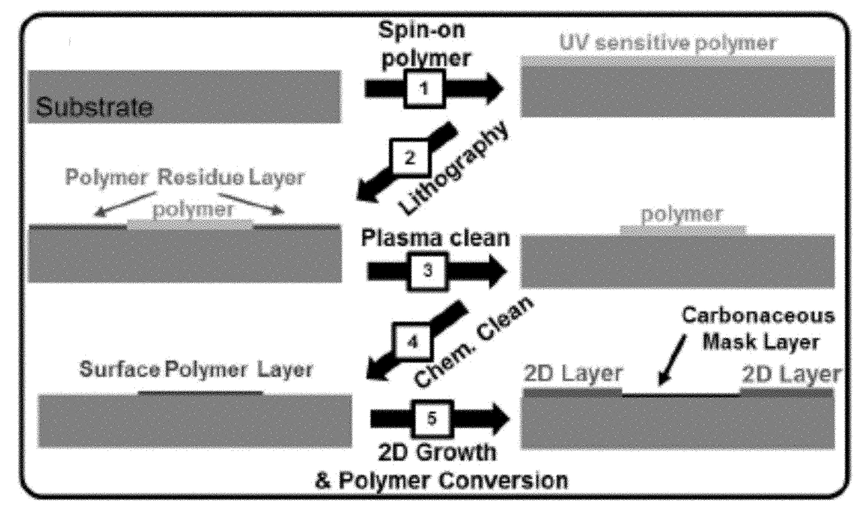
[0075]Heterogeneous integration of layered materials has been predicted to lead to completely new electronic properties (FIG. 3), resulting in novel electronic material entirely different from the constituent layers. Developing routes for templated growth will significantly enhance the ability to tune the electronic properties of these 2D materials. In spite of the predicted extraordinary properties of 2D nanoribbons, bottom-up template synthesis processes have been quite limited. Described herein is a novel method for bottom-up template synthesis of 2D materials.

Roughening of Substrate Surface does not Allow for Selective Growth

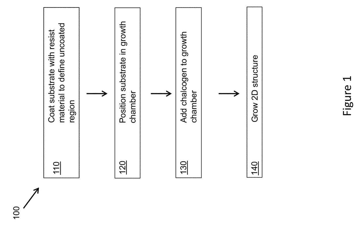
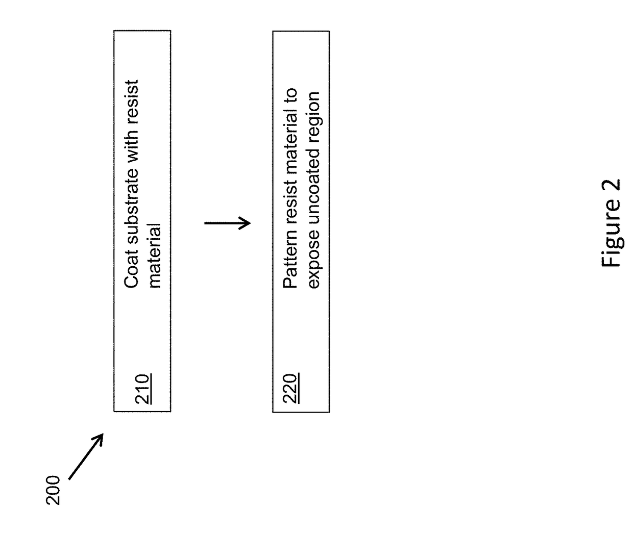
[0076]It was hypothesized that roughening of a substrate surface will enhance nucleation and growth rate of the layered material in those regions where the roughness is increased, thereby providing a means to grow in pre-patterned areas. To test this hypothesis, it was determined if one could se...

example 2

Area Growth of Two-Dimensional Materials

[0087]The data presented herein demonstrates the ability to selectively synthesize TMDs via substrate surface functionalization. These data experimentally demonstrate the robust templated growth of various semiconducting TMDs via conventional lithographic techniques and experimentally evaluate the surface chemistries in order to understand the exact functionalization responsible for selected area growth control. Lastly, top-gated field effect transistors were successfully fabricated and measured on selectively-grown chemical vapor deposited monolayer molybdenum disulfide (MoS2) on sapphire substrates for the first time.

[0088]The materials and methods employed in these experiments are now described.

Substrate Patterning

[0089]Substrates are cleaned in a standard procedure by sonication in acetone and IPA solvents followed by Nanostrip etch (Piranha solution: sulfuric acid / hydrogen peroxide) for 30 mins at 90° C. to remove organic contaminants and...


PUM

PropertyMeasurementUnit
Structureaaaaaaaaaa

Abstract

The present invention relates to methods for fabricating a laterally-limited two-dimensional structure through template synthesis. The methods of the invention are useful in forming homogenous and heterogeneous layered materials. The invention also provides structures and devices formed by the method of the present invention and uses thereof.

Description

CROSS-REFERENCE TO RELATED APPLICATIONS[0001]This application is a non-provisional of U.S. Provisional Patent Application Ser. No. 62 / 270,277, filed Dec. 21, 2015, the entire content of which is incorporated herein by reference.STATEMENT REGARDING FEDERALLY SPONSORED RESEARCH OR DEVELOPMENT[0002]This invention was made with government support under Contract No. HR0011-13-3-0002, awarded by The Department of Defense / Defense Advanced Research Projects Agency. The Government has certain rights in the invention.BACKGROUND OF THE INVENTION[0003]The isolation of graphene (one atomic layer of carbon) (Novoslev et al., 2005, Nature 438:197-200) constitutes a new paradigm in materials exploration in which atomic layer control is possible, (Avouris et al., 2012, Int Electron Devices Meet 23.1.1-4) and even though graphene is considered transformational, it is only the “tip of the iceberg.” Synthesizing and heterogeneously combining atomic layered transition metal dichalcogenides (Wang et al.,...

Claims


Application Information

Patent Timeline
IPC IPC(8): C23C16/04C23C14/04C23C16/02C23C14/02C23C16/18C23C14/22
CPCC23C16/04C23C16/18C23C14/04C23C16/0272C23C14/024C23C14/22C23C14/042C23C14/0623C23C16/042C23C16/305
Inventor ROBINSON, JOSHUA ALEXANDEREICHFELD, SARAH MARIEPIASECKI, ALEKSANDER FELIPEBERSCH, BRIAN MICHAEL
Owner PENN STATE RES FOUND
Why Eureka
Try Eureka