Microelectromechanical probe, method of manufacturing the same and probe set

Inactive Publication Date: 2017-06-22
MICROELECTRONICS TECH INC
View PDF2 Cites 3 Cited by
  • Summary
  • Abstract
  • Description
  • Claims
  • Application Information

AI Technical Summary

Benefits of technology

The present invention provides a microelectromechanical probe with a smaller pinpoint portion, which makes smaller probe marks on the device under test (DUT) and easier to pierce the passivation layer. The probe is made by a MEMS manufacturing process and then cut to form the cutting face and cut off a part of the pinpoint portion. The cut marks are formed in a way that a plurality of probes can be cut in a same cutting process. The method is favorable for batch and mass production. A sacrificial layer is formed on the substrate to stably fix the probe body and prevent displacement and deformation during the cutting process. The cutting direction is inclined relative to the probing direction to improve the image recognition in the automatic pinpoint recognition process. The invention also provides a probe set with two microelectromechanical probes with a rear side opposite to the cutting face, which makes the distance between the probing ends of two adjacent probes relatively smaller, to meet the fine pitch requirement of usage.

Problems solved by technology

However, the MEMS manufacturing process causes a restriction on the shape of the probe 10.
Such probing end 135 has disadvantages of making relatively larger probe marks on the DUT and having less recognizable image in the automatic pinpoint recognition process.
Besides, the probing end 135 may be not sharp enough to pierce the passivation layer on the surface of the DUT, causing undesired faults or errors in testing the DUT.

Method used


Image

  • Microelectromechanical probe, method of manufacturing the same and probe set
  • Microelectromechanical probe, method of manufacturing the same and probe set
  • Microelectromechanical probe, method of manufacturing the same and probe set

Examples


Embodiment Construction

[0038]First of all, it is to be mentioned that same reference numerals used in the following preferred embodiments and the appendix drawings designate same or similar elements throughout the specification for the purpose of concise illustration of the present invention.

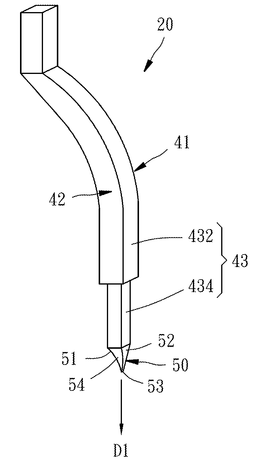
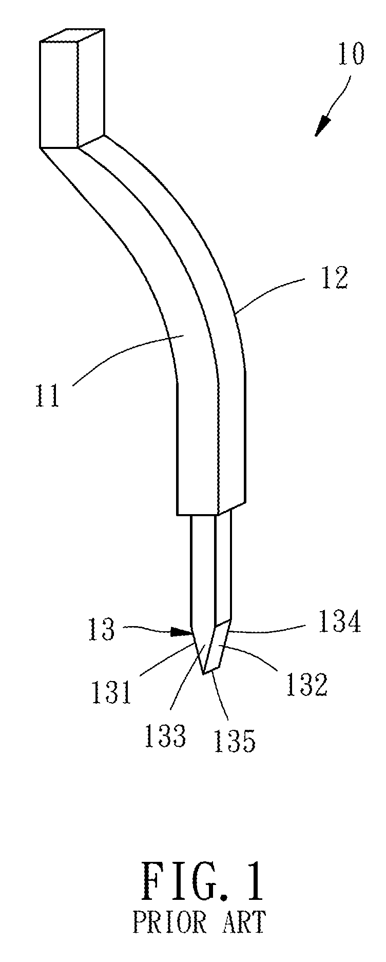
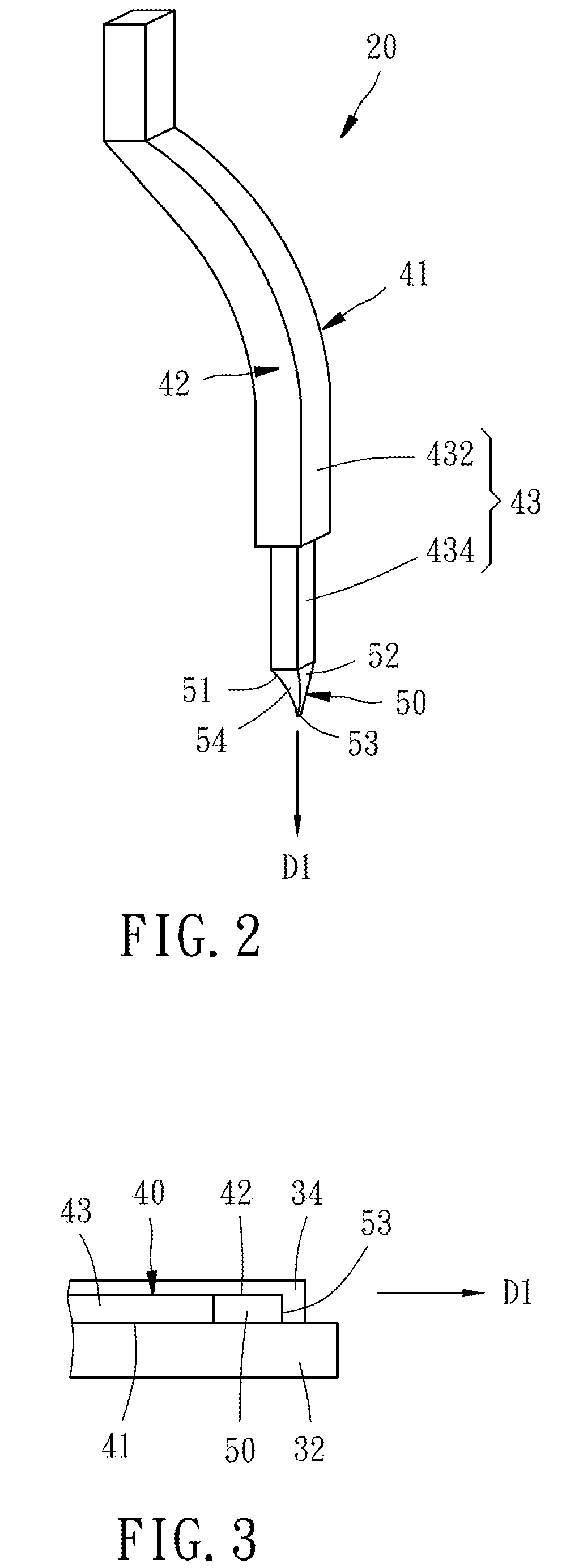
[0039]Referring to FIG. 2, a microelectromechanical probe 20 according to a first preferred embodiment of the present invention is similar to the conventional buckling probe 10 made by the MEMS manufacturing process as shown in FIG. 1, but has a difference in the configuration of the pinpoint portion therebetween. The method of manufacturing the microelectromechanical probe 20 will be described in the following paragraphs, and the structural features of the microelectromechanical probe 20 will be described at the same time. The method of manufacturing the microelectromechanical probe 20 includes the following steps.

[0040]a) As shown in FIG. 3, perform a MEMS manufacturing process to form a probe body 40 (like the prob...


PUM

PropertyMeasurementUnit
Angleaaaaaaaaaa
Angleaaaaaaaaaa
Angleaaaaaaaaaa

Abstract

A microelectromechanical probe is manufactured by a MEMS manufacturing process forming a probe body and a cutting process providing a pinpoint portion a cutting face. The probe has a top surface, a body portion, and a pinpoint portion extended in a probing direction from the body portion and provided with first and second sides and a probing end oriented in the probing direction. The cutting face is provided on the top surface, adjoins the first and second sides and the probing end, and has at least one cut mark formed by the cutting process, extended from the first side to the second side and non-parallel to the probing direction. The cutting face descends from an edge cut mark to the probing end.

Description

BACKGROUND OF THE INVENTION[0001]1. Field of the Invention[0002]The present invention relates generally to a probe used in a probe card for probing a device under test (hereinafter referred to as “DUT”), and more particularly to a microelectromechanical probe, a method of manufacturing the microelectromechanical probe, and a probe set using the microelectromechanical probe.[0003]2. Description of the Related Art[0004]FIG. 1 shows a conventional buckling probe 10, namely cobra probe, which is manufactured by a microelectromechanical system manufacturing process (hereinafter referred to as “MEMS manufacturing process”). In the manufacturing process, the buckling probe 10 is formed on a substrate (not shown) with a lying posture on the substrate. Specifically speaking, before the buckling probe 10 is completely formed, a photoresist layer is formed on the substrate and then defined by a photomask and developed with a hollow pattern by photolithography technique in a way that the hollow...

Claims


Application Information

Patent Timeline
IPC IPC(8): G01R1/073B81C1/00B81B1/00
CPCG01R1/07357B81C1/00007B81B1/008G01R1/06738G01R1/06744G01R3/00
Inventor WEI, SHAO-LUNHSU, YU-CHENSHEN, MAO-FAHSU, CHIH-HAO
Owner MICROELECTRONICS TECH INC
Why Eureka
Try Eureka