Semiconductor memory device and method for detecting weak cells

Active Publication Date: 2017-06-22
SK HYNIX INC
View PDF10 Cites 17 Cited by
  • Summary
  • Abstract
  • Description
  • Claims
  • Application Information

AI Technical Summary

Benefits of technology

[0010]Various embodiments are directed to a semiconductor memory device capable of detecting and screening weak cells using a power scheme of a word line driving circuit without a sepa

Problems solved by technology

When such a method is applied, most errors are detected.
However, so-called weak cells of which one bit or several bits are dead due to charge sharing may not be detected.
According to

Method used


Image

  • Semiconductor memory device and method for detecting weak cells
  • Semiconductor memory device and method for detecting weak cells
  • Semiconductor memory device and method for detecting weak cells

Examples


Embodiment Construction

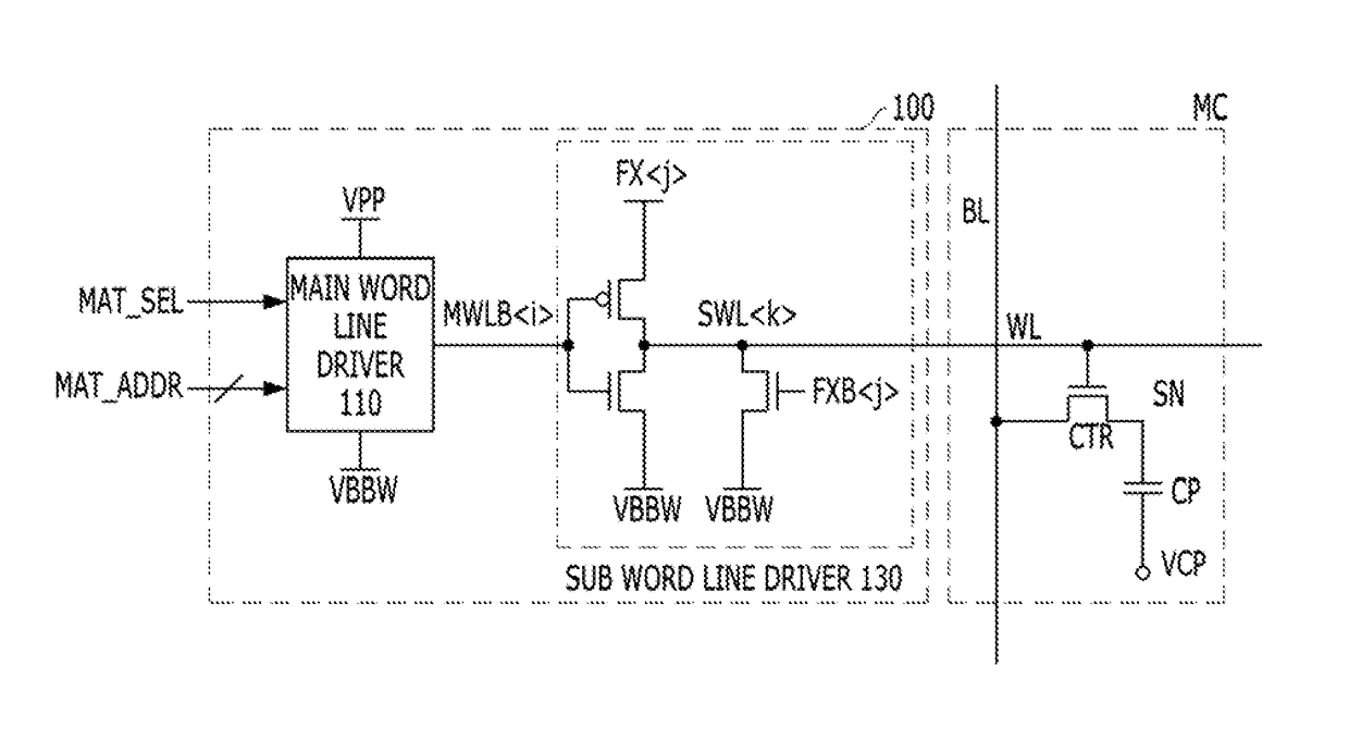
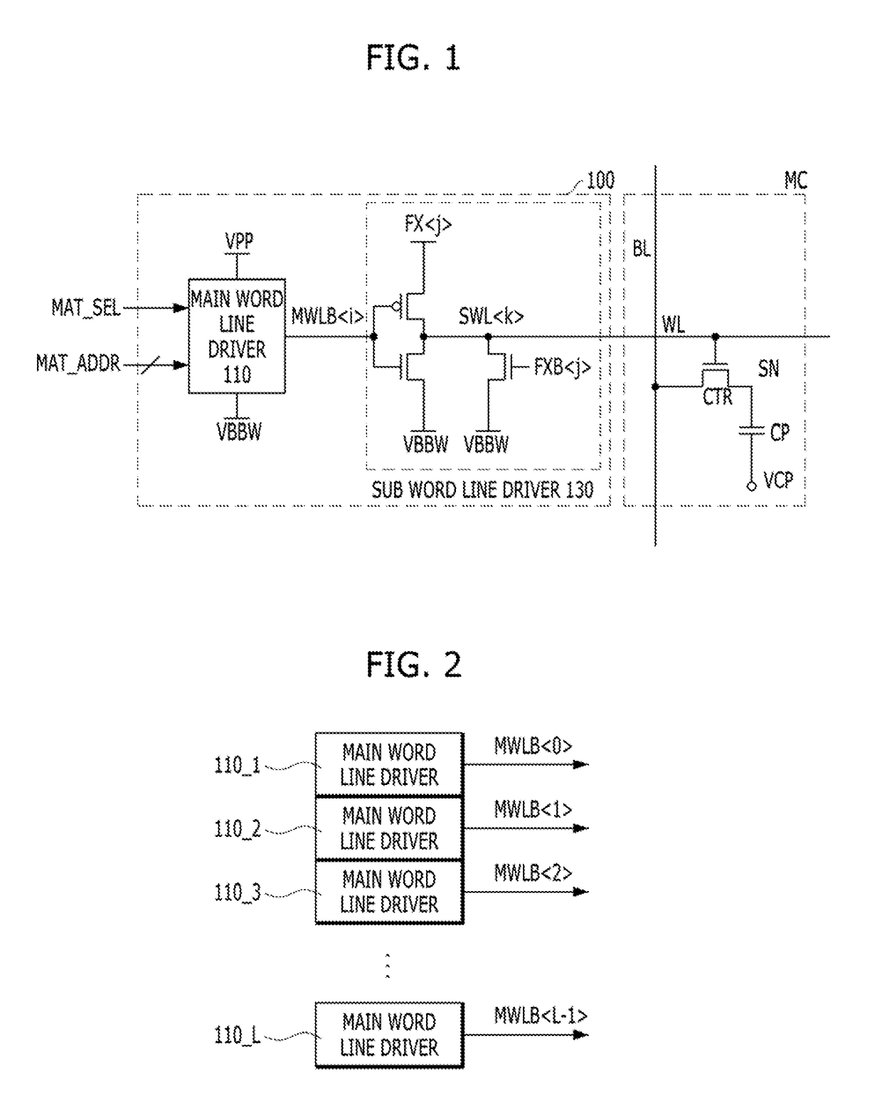
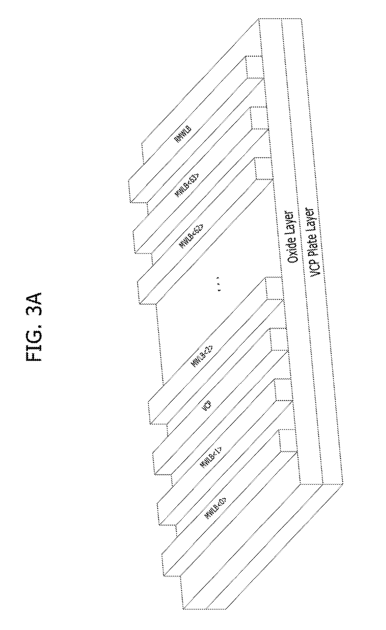
[0023]Various embodiments will be described below in more detail with reference to the accompanying drawings. The present invention may, however, be embodied in different forms and should not be construed as being limited to the embodiments set forth herein. Rather, these embodiments are provided so that this disclosure will be thorough and complete, and will fully convey the present invention to those skilled in the relevant art. Throughout the disclosure, like reference numerals refer to like parts throughout the various figures and embodiments of the present invention. It is also noted that in this specification, “connected / coupled” refers to one component not only directly coupling another component but also indirectly coupling another component through an intermediate component. It will be understood that, although the terms “first”, “second”, “third”, and so on may be used herein to describe various elements, components, regions, layers and / or sections, these elements, compone...


PUM


Abstract

A semiconductor memory device may include: a memory cell array coupled between a plurality of word lines and a plurality of bit lines; a first source voltage supply unit suitable for providing a boosted voltage to a source voltage terminal when a cell mat signal is activated; a second source voltage supply unit suitable for providing a dropped voltage that is lower than the boosted voltage to the source voltage terminal; a word line driving circuit suitable for selecting one of the plurality of word lines in response to an address combination signal and driving the selected word line and unselected word lines, when the cell mat signal is activated; and a weak cell detection circuit suitable for detecting a weak cell by checking data values of memory cells coupled to a word line which is driven by the word line driving circuit during the test mode.

Description

CROSS-REFERENCE TO RELATED APPLICATIONS[0001]The present application claims priority of Korean Patent Application No. 10-2015-0179960, filed on Dec. 16, 2015, which is incorporated herein by reference in its entirety.BACKGROUND[0002]1. Field[0003]This patent document relates to semiconductor design technology and, more particularly, to a semiconductor memory device including a word line driving circuit and a method for detecting weak cells therein.[0004]2. Description of the Related Art[0005]Typically, after a semiconductor memory device is designed and fabricated, a test process at the wafer level and a test process at the package level are performed to determine whether the semiconductor memory device includes any chip fails.[0006]During the wafer level test, a large amount of data is tested at a time through 64 or 128 parallel channels. Furthermore, since an operating frequency during the wafer level test is basically low, without considering an external noise or a noise caused b...

Claims


Application Information

Patent Timeline
IPC IPC(8): G11C29/50G01R31/3181
CPCG01R31/3181G11C29/50004G11C8/08G11C2029/1204G11C29/50G06F2201/81
Inventor CHOI, YOUNG-GEUN
Owner SK HYNIX INC
Why Eureka
Try Eureka