Semiconductor device

a technology of semiconductors and devices, applied in the direction of semiconductor/solid-state device details, pulse techniques, diodes, etc., can solve the problems of easy breakdown of semiconductors, failures, and easy transient and local high temperature, and achieve relatively small heat generation, favorable suppression of temperature rise, and relatively high dynamic clamping capability

Active Publication Date: 2017-06-22
ROHM CO LTD
View PDF4 Cites 9 Cited by
  • Summary
  • Abstract
  • Description
  • Claims
  • Application Information

AI Technical Summary

Benefits of technology

[0011]In the semiconductor device according to the present invention, the first functional element forming region is configured such that the area of a channel forming region per unit area is relatively small compared to the area of the second functional element forming region. That is, the first functional element forming region is configured such that the amount of heat generation is relatively small, and thus the dynamic clamping capability is relatively high. As such, the first functional element forming region is provided at the region where heat generation should be suppressed, thereby favorably suppressing a temperature rise, while increasing dynamic clamping capability.
[0012]On the other hand, the second functional element forming region is configured such that the area of a channel forming region per unit area is relatively large compared to the area of the first functional element forming region. Accordingly, in the second functional element forming region, a current path having a relatively wide area can be secured with the channel forming region having a relatively large area, and therefore the current path can be prevented from decreasing as a whole in the presence of both the first functional element forming regions and the second functional element forming regions. Thereby, the increase in on-resistance can be suppressed.
[0013]As described above, according to the semiconductor device of the present invention, the temperature increase can be suppressed by optimizing the layout of the channel forming regions. Further, according to the semiconductor device of the present invention, it is possible to increase dynamic clamping capability while suppressing an increase in on-resistance.

Problems solved by technology

With this configuration, the heat generated along both the lateral sides of the trenches may interact with each other at the entire region along both the lateral sides of the trenches, and therefore there is a problem that a portion of a substrate is easily subjected to high temperature transiently and locally.
If the energy applied to the semiconductor device from the inductive load exceeds a prescribed level, the breakdown of the semiconductor may take place due to temperature rise.
According to the semiconductor device as shown in the patent literature 1, a portion of the substrate is possibly subjected to high temperature transiently and locally when receiving the energy from the inductive load, and thus failures might easily take place at the portion, and therefore there is a problem that the semiconductor device can no longer absorb the energy stored in the inductive load.
As a result, it is difficult to achieve favorable dynamic clamping capability.
However, in this case, there is a trade-off problem, that is, if the area of a channel forming region decreases, an on-resistance increases.

Method used


Image

  • Semiconductor device
  • Semiconductor device
  • Semiconductor device

Examples


first embodiment

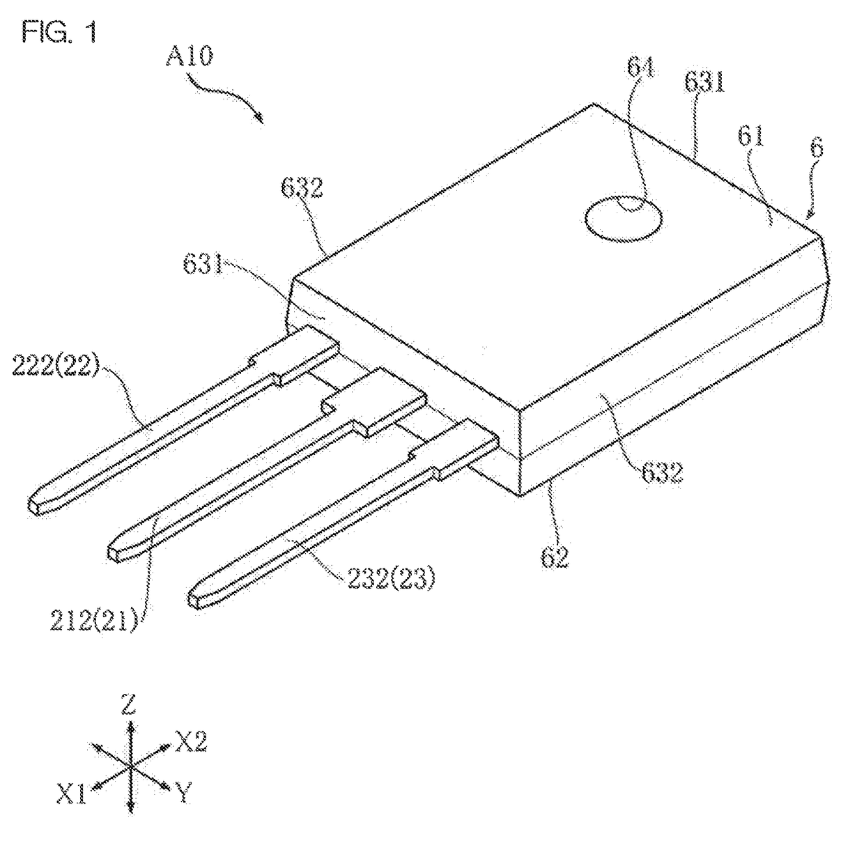
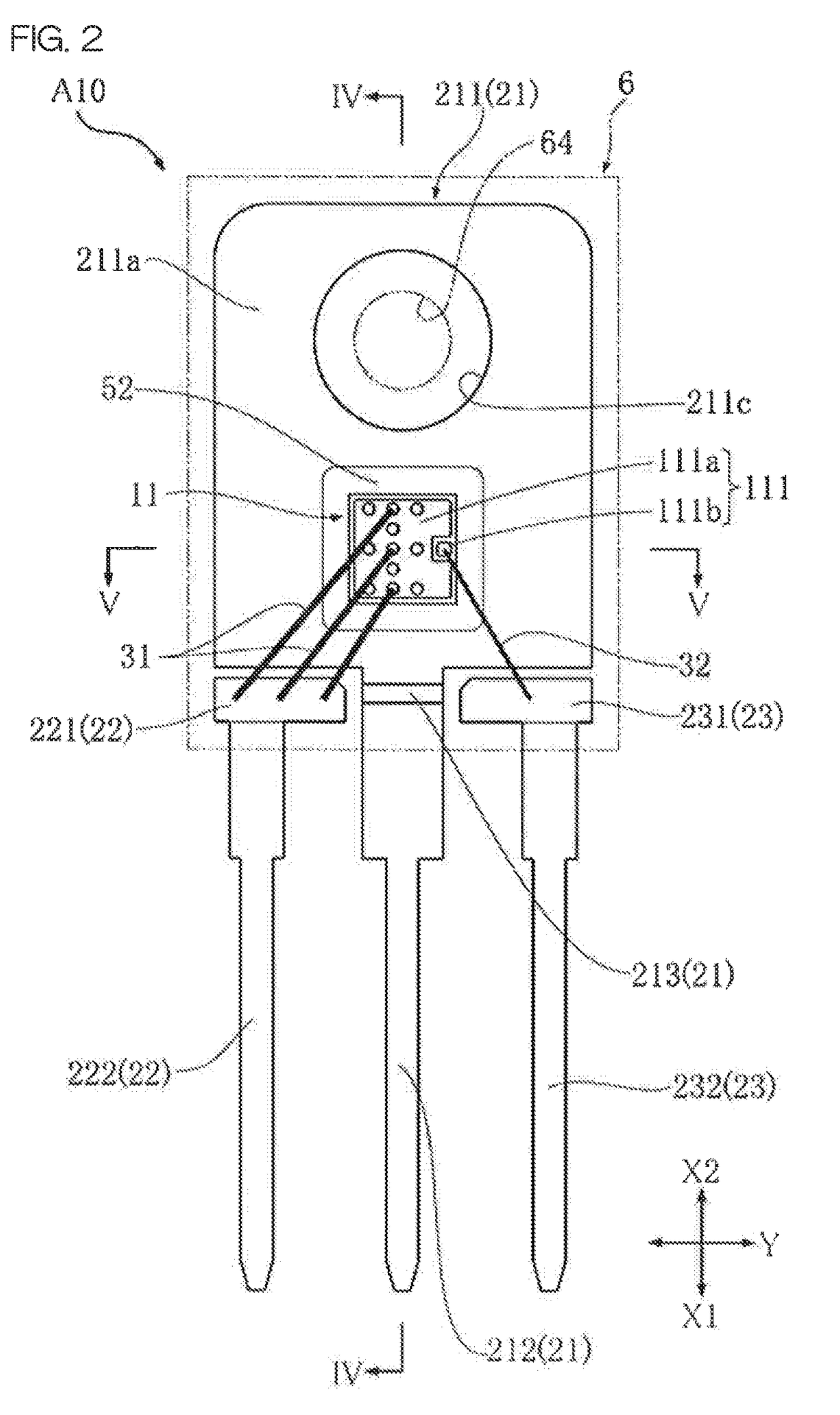
[0043]A semiconductor package A10 according to a first embodiment of the present invention is described on the basis of FIGS. 1 to 8. The semiconductor package A10 includes a semiconductor device 11, a junction layer 12, a first lead 21, a second lead 22, a third lead 23, a first bonding wire 31, a second bonding wire 32, a plurality of heat releasing member 4, an externally plated layer 51, an internally plated layer 52, and a sealing resin 6. Hereinafter, the semiconductor package A10 may be referred to as a semiconductor device A10, and the semiconductor device 11 may be referred to as a semiconductor element 11.

[0044]FIG. 1 is a perspective view of a semiconductor package A10. FIG. 2 is a plan view of the semiconductor package A10. FIG. 3 is a bottom view of the semiconductor package A10. FIG. 4 is a cross-sectional view taken along the line IV-IV shown in FIG. 2. FIG. 5 is a cross-sectional view taken along the line V-V shown in FIG. 2. FIG. 6 is a plan view of a major part of ...

second embodiment

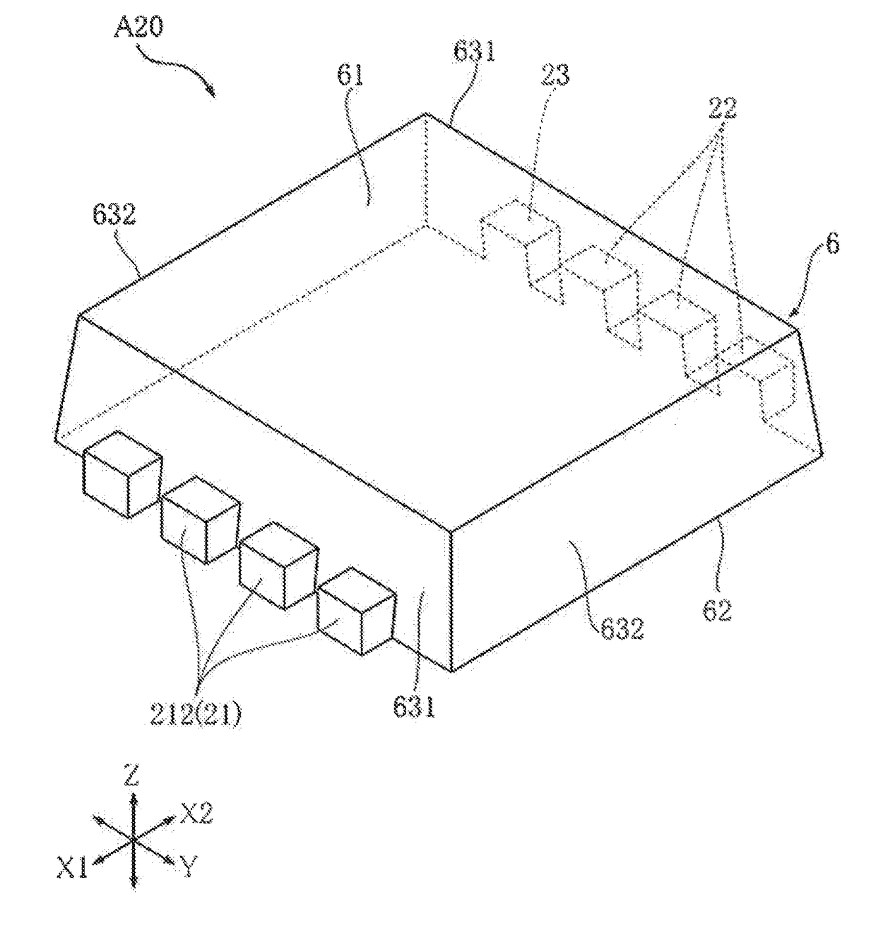
[0078]Description is made for a semiconductor package A20 according to a second embodiment of the present invention with reference to FIGS. 9 to 14. In these drawings, the same reference numerals are applied to the same or similar elements as those in the semiconductor package A10 described above to thereby avoid duplicate descriptions.

[0079]FIG. 9 is a perspective view of the semiconductor package A20. FIG. 10 is a plan view of the semiconductor package A20. FIG. 11 is a bottom view of the semiconductor package A20. FIG. 12 is a cross-sectional view taken along the line XII-XII (dashed-dotted line) shown in FIG. 10. FIG. 13 is a cross-sectional view taken along the line XIII-XIII shown in FIG. 10. FIG. 14 is a plan view of a major part of the semiconductor device 11 in the semiconductor package A20. The sealing resin 6 is omitted in FIG. 10 for the sake of understanding. The sealing resin 6 omitted in FIG. 10 is shown by an imaginary line (two-dot chain line).

[0080]The semiconducto...


PUM


Abstract

A semiconductor device according to the present invention includes: a substrate; a plurality of trenches formed in the substrate; and a plurality of functional element forming regions arrayed along each of the trenches, including a channel forming region as a current path, wherein the plurality of functional element forming regions includes a first functional element forming region in which the area of the channel forming region per unit area is relatively small and a second functional element forming region in which the area of the channel forming region per unit area is relatively large, and the first functional element forming region is provided at a region where heat generation should be suppressed.

Description

CROSS-REFERENCE TO RELATED APPLICATIONS[0001]This application corresponds to, Patent Application No. 2015-245307 submitted to Japanese Patent Office on Dec. 16, 2015, Patent Application No. 2016-24524 submitted to Japanese Patent Office on Feb. 12, 2016, and Patent Application No. 2016-202761 submitted to Japanese Patent Office on Oct. 14, 2016, the entire contents of these applications are hereby incorporated by reference.TECHNICAL FIELD[0002]The present invention relates to a semiconductor device.BACKGROUND ART[0003]A patent literature 1 (Japanese Unexamined Patent Application Publication 2010-267677) discloses a semiconductor device equipped with a trench gate type Metal Oxide Semiconductor Field Effect Transistor (MOSFET). The semiconductor device includes a semiconductor substrate in which a plurality of trenches is formed, a gate electrode embedded in the trenches with a gate insulating film sandwiched therebetween, and an n-type source region, a p-type body region, and n-type...

Claims


Application Information

Patent Timeline
Patent Type & Authority Applications(United States)
IPC IPC(8): H01L27/02H01L23/373H01L23/31H01L29/78H01L23/498
CPCH01L27/0255H01L29/7827H01L23/3736H01L23/49838H01L23/3171H01L23/49811H01L2924/181H01L2224/0603H01L2224/32245H01L2224/48247H01L2224/4903H01L2224/49111H01L23/3107H01L23/4334H01L23/4952H01L23/49562H01L29/66348H01L29/7397H01L29/0696H01L29/1095H03K17/08122H03K2017/0806H01L29/7813H01L29/66734H01L2224/73265H01L2224/48091H01L2924/18301H01L2924/00012H01L2924/00014H03K17/00
Inventor OKUDA, HAJIMEHAGA, MOTOHARUFUJII, KENJI
Owner ROHM CO LTD
Why Eureka
Try Eureka