Semiconductor device and display device including the same

a technology of semiconductor devices and display devices, which is applied in semiconductor devices, electrical equipment, instruments, etc., can solve the problems of increasing the power consumption of display devices due to continuous supply of bias voltages, and achieve the effects of reducing power consumption, favorable visibility, and favorable visibility

Inactive Publication Date: 2017-06-22
SEMICON ENERGY LAB CO LTD
View PDF0 Cites 28 Cited by
  • Summary
  • Abstract
  • Description
  • Claims
  • Application Information

AI Technical Summary

Benefits of technology

[0028]According to another embodiment of the present invention, a semiconductor device with reduced power consumption, a display device including the semiconductor device, or a display module including the semiconductor device can be provided. According to another embodiment of the pres...

Problems solved by technology

In other words, continuous supply of the bias volta...

Method used


Image

  • Semiconductor device and display device including the same
  • Semiconductor device and display device including the same
  • Semiconductor device and display device including the same

Examples


embodiment 1

[0068]In this embodiment, a source driver circuit and a bias generator included in the source driver circuit are described.

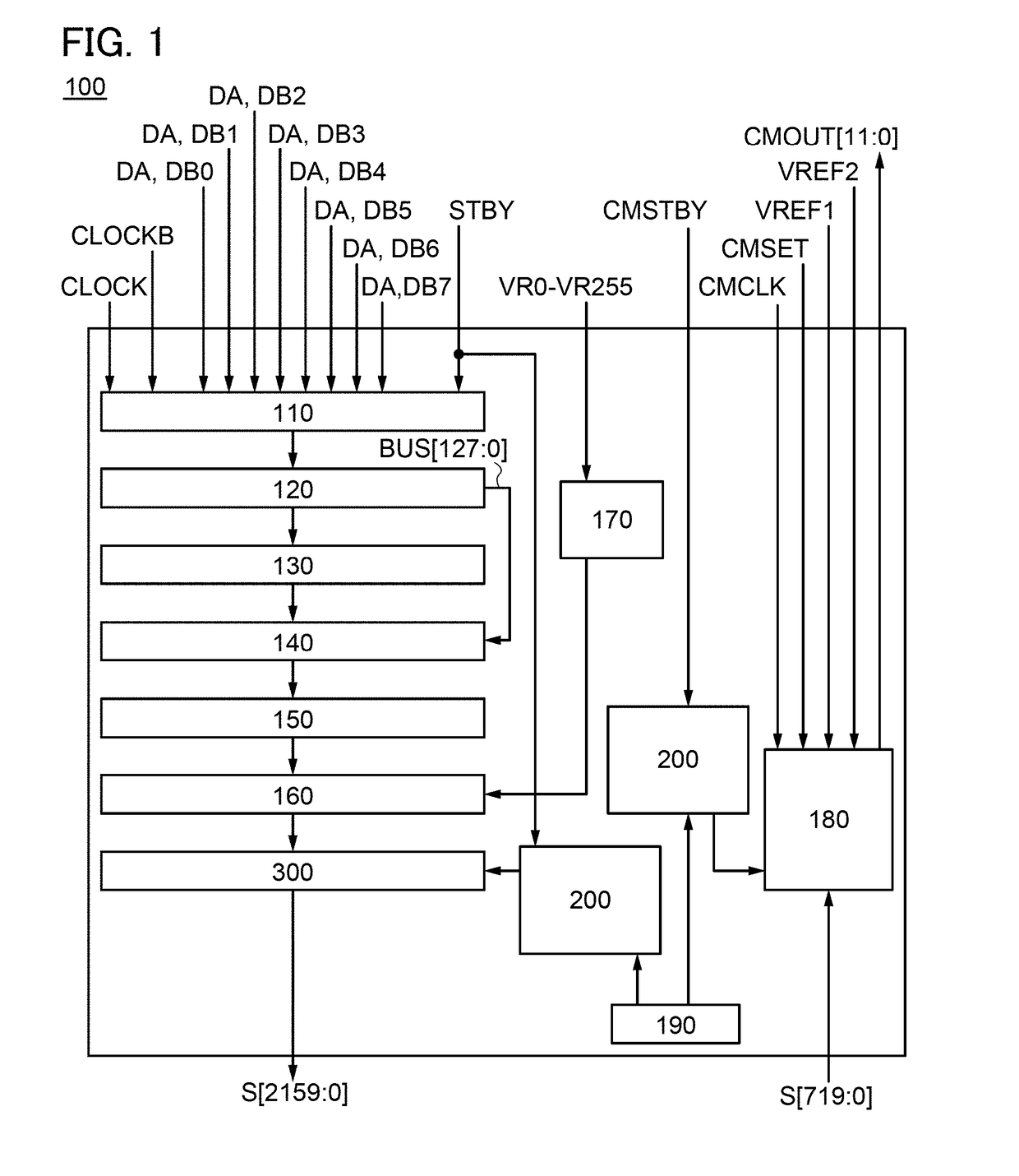
[0069]FIG. 1 illustrates an example of a source driver circuit of one embodiment of the present invention. A source driver circuit 100 includes a low voltage differential signaling (LVDS) receiver 110, a serial-parallel converter circuit 120, a shift register circuit 130, latch circuits 140, a level shifter circuit 150, a pass transistor logic circuit 160, a resistor string circuit 170, an external correction circuit 180, a band gap reference (BGR) circuit 190, bias generators 200, and a buffer amplifier 300. Note that the number of the bias generators 200 included in the source driver circuit 100 in FIG. 1 is two.

[0070]The LVDS receiver 110 is electrically connected to an external host processor. The LVDS receiver 110 has a function of receiving video signals from the host processor and has a function of converting a differential signal to a single-end signal, ...

specific example 1

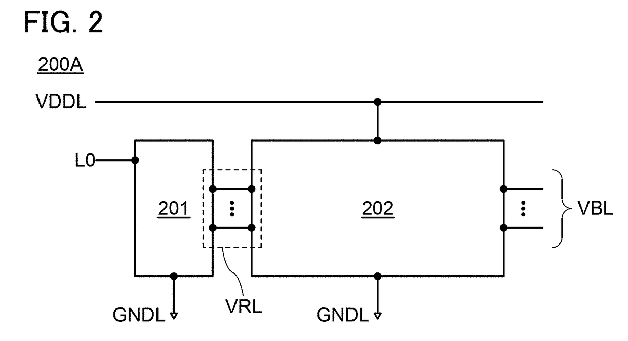
[0126]A bias generator 200B1, a specific circuit example for obtaining the bias generator 200B, is shown in FIG. 7.

[0127]The bias generator 200B1 is configured in such a manner that the circuit 203, the circuit 204, and the circuit 205 are incorporated in the bias generator 200A1. Therefore, the same contents as the bias generator 200A1 are not described and different points from the bias generator 200A1 are described.

[0128]Note that as for a different point from the bias generator 200B of FIG. 6, the circuit 202 includes the circuit 204 and the circuit 205 of the bias generator 200B1 of FIG. 7. Since the circuit 204 and the circuit 205 only need be electrically connected to the plurality of wirings VBL, the circuit 204 and the circuit 205 may be included in the circuit 202. In other words, one embodiment of the present invention is not limited to the configuration of the bias generator 200B shown in FIG. 6, and the configuration of the bias generator 200B shown in FIG. 6 may be cha...

operation example

[0136]Next, an operation example of the bias generator 200B1 is described. Note that the bias generator 200B1 operates in substantially the same manner as the bias generator 200A1; therefore, the description of the operation example of the bias generator 200A1 is referred to for operations of the bias generator 200B1 which are the same as those of the bias generator 200A1, and functions and operations which are obtained by providing the circuits 203 to 205 are described below.

[0137]As described above, when the display device displays a still image, bringing the buffer amplifier 300 and the bias generator 200 into a standby state (temporarily stopping the buffer amplifier 300 and the bias generator 200) can reduce the power consumption of the display device. The bias generator 200B1 can be brought into a standby state (temporarily stopped) by the operations of the circuits 203 to 205.

[0138]The bias generator 200B1 can be brought into either a driving state or a standby state (tempora...


PUM


Abstract

A semiconductor device with reduced power consumption and a display device including the semiconductor are provided. The semiconductor device generates a bias voltage that is to be supplied to a buffer amplifier. When the display device displays a still image, a data signal for updating the image need not be supplied from the buffer amplifier to a pixel array in the next frame; therefore, the circuit is configured so that the buffer amplifier is brought into a standby state (temporarily stopped). Specifically, input of a reference current from a BGR circuit to the semiconductor is stopped and a bias voltage is applied from the semiconductor device to the buffer amplifier to temporarily stop the operation of the buffer amplifier.

Description

TECHNICAL FIELD[0001]One embodiment of the present invention relates to a semiconductor device and a display device including the semiconductor device.[0002]Note that one embodiment of the present invention is not limited to the above technical field. The technical field of the invention disclosed in this specification and the like relates to an object, a method, or a manufacturing method. In addition, one embodiment of the present invention relates to a process, a machine, manufacture, or a composition of matter. Specifically, examples of the technical field of one embodiment of the present invention disclosed in this specification include a semiconductor device, a display device, a liquid crystal display device, a light-emitting device, a power storage device, an imaging device, a memory device, a processor, an electronic device, a method for driving any of them, a method for manufacturing any of them, a method for testing any of them, and a system including any of them.BACKGROUND...

Claims


Application Information

Patent Timeline
IPC IPC(8): H01L27/12G09G3/20
CPCH01L27/124H01L27/1251G09G3/2092G09G2330/028G09G2300/0809G09G2310/0286G09G2310/0291G09G2330/021G09G2300/0426G09G2300/0814G09G2300/0819G09G2300/0838G09G2300/0842G09G2300/0852H01L27/1225
Inventor TAKAHASHI, KEI
Owner SEMICON ENERGY LAB CO LTD
Why Eureka
Try Eureka