Method for fabricating semiconductor device including fin shaped structure

a technology of semiconductor devices and fins, which is applied in the direction of semiconductor devices, basic electric elements, electrical equipment, etc., can solve the problems that the layout design of finfet structures still faces some issues in conventional finfet fabrication, and achieve the effect of improving element performance and increasing carrier mobility

Active Publication Date: 2017-07-06
UNITED MICROELECTRONICS CORP
View PDF6 Cites 0 Cited by
  • Summary
  • Abstract
  • Description
  • Claims
  • Application Information

AI Technical Summary

Benefits of technology

[0005]It is one of the primary objectives of the present invention to provide a semiconductor device, which has a silicon germanium layer uniformly distributed in a fin shaped structure, so as to effectively improve the carrier mobility of the channel region thereof, as well as the element performance.
[0006]It is another one of the primary objectives of the present invention to provide a method of forming the semiconductor device, in which a silicon germanium layer may be formed uniformly in at least 80% to 90% of the fin shaped structure, so that, the method is able to improve the carrier mobility of the channel region in the semiconductor device, as well as the element performance thereof.
[0009]According to the above, the semiconductor device and the forming method thereof in the present invention mainly form an epitaxial layer on surfaces of the silicon-containing substrate and the fin shaped structures, and then perform a germanium condensation process. In this way, the epitaxial layer may react with oxygen to form an oxide layer, and the epitaxial layer may also experience condensation simultaneously, thereby driving the germanium inwardly into the fin shaped structures and the substrate. Thus, a great amount of germanium from the epitaxial layer may accumulate in the fin shaped structures and the substrate, such that, a silicon germanium layer may be formed accordingly in the fin shaped structures and the substrate. Thus, the semiconductor device of the present invention is able to stress the channel region of a semiconductor transistor formed subsequently due to the relative higher lattice constant of the silicon germanium layer in comparison with the silicon substrate, so that the present invention may achieve the purpose of increasing the carrier mobility and improving the element performance.

Problems solved by technology

However, layout designs of the FinFET structures still face some issues in conventional FinFET fabrication.

Method used


Image

  • Method for fabricating semiconductor device including fin shaped structure
  • Method for fabricating semiconductor device including fin shaped structure
  • Method for fabricating semiconductor device including fin shaped structure

Examples


first embodiment

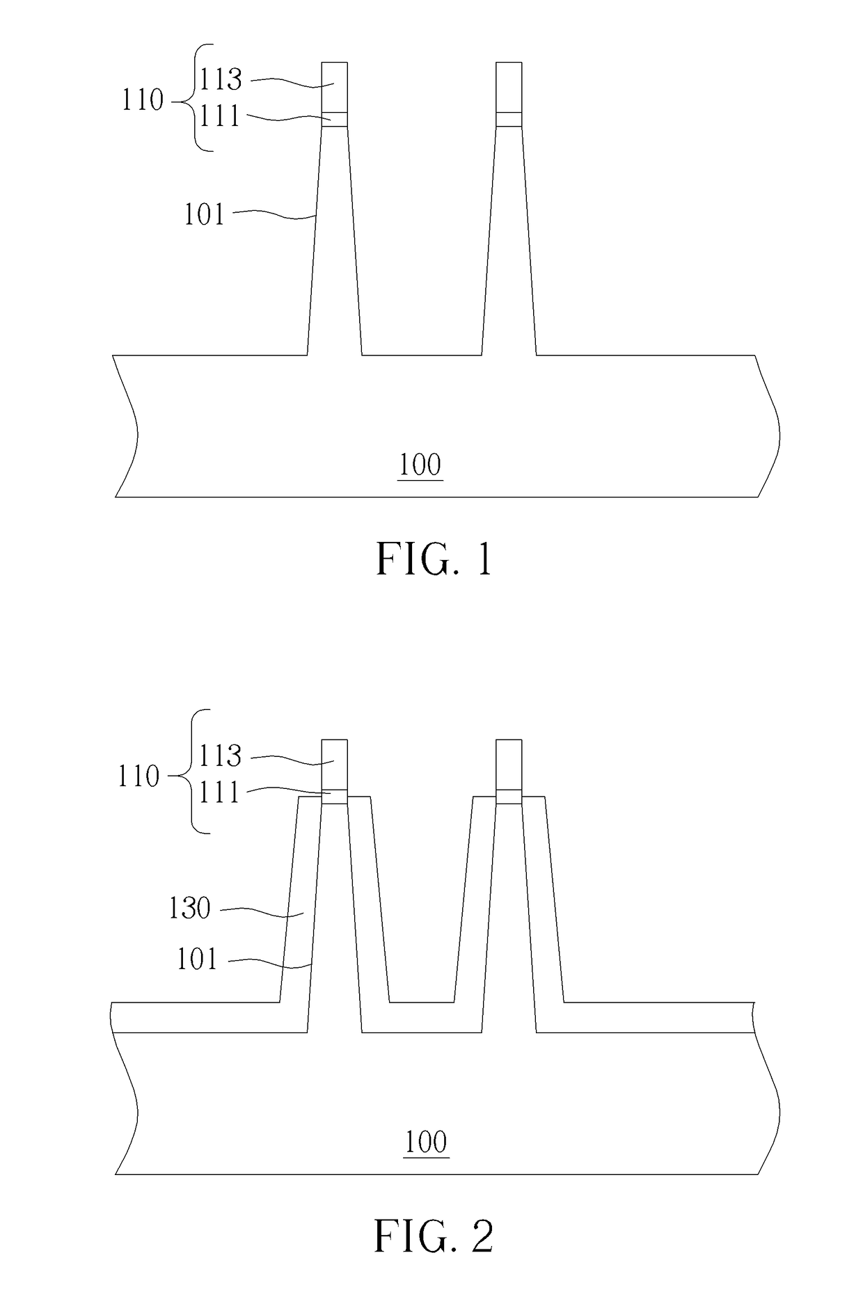
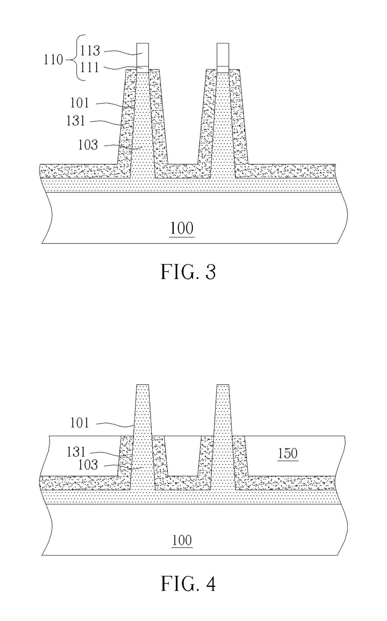
[0024]Please refer to FIG. 1 to FIG. 5, which are schematic diagrams illustrating a method of forming a semiconductor device according to the present invention. First of all, a substrate 100 is provided, for example including a semiconductor substrate, such as a silicon substrate, a silicon-containing substrate or a silicon-on-insulator (SOI) substrate, and at least one fin shaped structure 101 is formed on the substrate 100. In the embodiment of having the bulk silicon, the formation of the fin shaped structure 101 may include a spacer self-aligned double-patterning (SADP) process, also known as sidewall image transfer (SIT) process. The SADP process may include forming a plurality of patterned sacrificial layers (not shown in the drawings) on the substrate 100 by using a photolithography and etching process, performing a depositing and etching processes sequentially to form a spacer (not shown in the drawings) at sidewalls of each of the patterned sacrificial layers, and then remo...

second embodiment

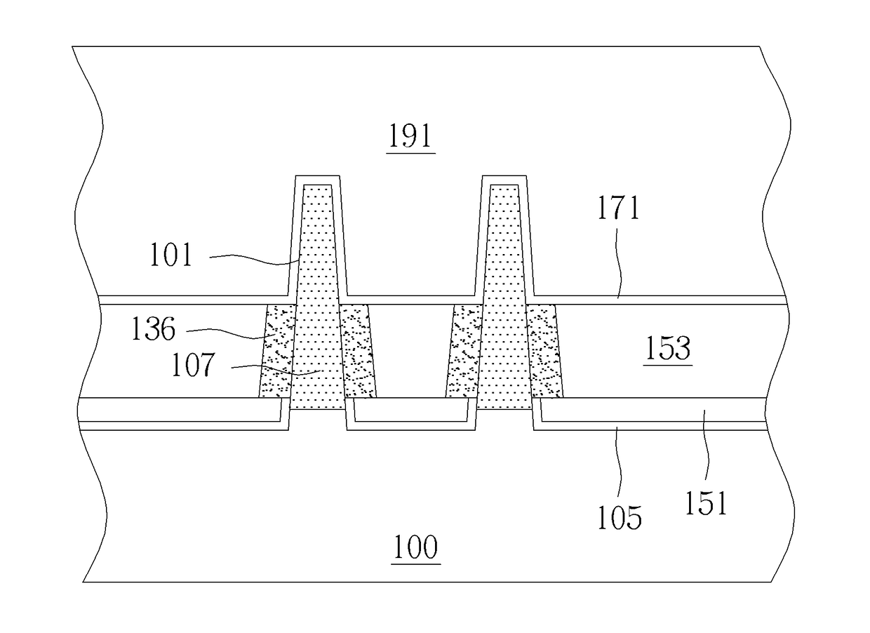
[0042]According to above mentioned steps, the semiconductor device according to the present invention is obtained. In the following, the method of the present invention may be integrated with a general gate forming process, to pattern the gate dielectric layer 171 and the gate layer 191, thereby forming a gate structure (not shown in the drawings) across the fin shaped structures 101. Otherwise, a source / drain selective epitaxial growing (SEG) process, a silicidation process, a contact etching stop layer (CESL) process or a replacement metal gate (RMG) process may be performed subsequently. Those processes are similar to a conventional forming process of a transistor and will not be further detailed herein. In the method of the present embodiment, the shallow trench isolation is formed partially both before and after the epitaxial layer is formed, such that, the epitaxial layer only disposed on the surfaces of the fin shaped structures may be formed accordingly. In this manner, the ...


PUM


Abstract

A semiconductor device and a method of fabricating the same, the semiconductor device includes a silicon substrate, a fin shaped structure and a shallow trench isolation. The fin shaped structure is disposed on the silicon substrate and includes a silicon germanium (SiGe) layer extending from bottom to top in the fin shaped structure. The shallow trench isolation covers a bottom portion of the fin shaped structure.

Description

CROSS REFERENCE TO RELATED APPLICATIONS[0001]This application is a Continuation of application Ser. No. 14 / 855,390 filed Sep. 16, 2015, and included herein by reference.BACKGROUND OF THE INVENTION1. Field of the Invention[0002]The invention relates to a method of fabricating a semiconductor device, and more particularly, to a method of fabricating a semiconductor device having a silicon germanium (SiGe) epitaxial structure.2. Description of the Prior Art[0003]With the trend in the industry being scaling down the size of the field effect transistors (FETs), three-dimensional or non-planar transistor technology, such as fin field effect transistor technology (FinFET) has been developed to replace planar FETs. Since the three-dimensional structure of a FinFET increases the overlapping area between the gate and the fin shaped structure of the silicon substrate, the channel region can therefore be more effectively controlled. This way, the drain-induced barrier lowering (DIBL) effect and...

Claims


Application Information

Patent Timeline
Patent Type & Authority Applications(United States)
IPC IPC(8): H01L21/762H01L29/161H01L29/66H01L29/06H01L21/02H01L29/78
CPCH01L21/76224H01L21/02532H01L29/161H01L29/66795H01L29/0649H01L29/785H01L21/02656H01L29/7855H01L29/1054H01L29/7848H01L29/7851H01L29/7849
Inventor CHIU, CHUNG-YIHONG, SHIH-FANGLIN, CHAO-HUNG
Owner UNITED MICROELECTRONICS CORP
Why Eureka
Try Eureka