Majority current assisted radiation detector device

a detector device and majority current technology, applied in the direction of reradiation control devices, instruments, instruments, etc., can solve the problems of consuming valuable pixel optical area, unable to use other things, and unable to achieve the shrinking of pixel pitch, so as to achieve the effect of reducing the size of the devi

Active Publication Date: 2017-07-06
SOFTKINETIC SENSORS
View PDF0 Cites 27 Cited by
  • Summary
  • Abstract
  • Description
  • Claims
  • Application Information

AI Technical Summary

Benefits of technology

[0018]In the case of a BSI implementation, the semiconductor region located between the two detection regions, being a well or a deep well, can be arranged for receiving pixel circuitry elements. This is really advantageous, because the size of the device can be considerably reduced, while ensuring the insulation of the detection regions.

Problems solved by technology

This requirement involves high power consumption; this is one of the main drawbacks of CAPDs.
In a conventional CAPD implementation as shown in FIG. 2 A-C and FIG. 3, reduction in power consumption is typically achieved by separating the nodes by high-ohmic epitaxial layer (for example doped p−−) which, as a consequence, consumes valuable pixel optical area and renders the shrinking of the pixel pitch challenging.
The separation requirement means space that cannot be used for other things such as pixel transistors.
Therefore, in conventional CAPDs reducing the pixel pitch remains very challenging when coupled with a device specification targeting low power consumption and high fill factor.

Method used


Image

  • Majority current assisted radiation detector device
  • Majority current assisted radiation detector device
  • Majority current assisted radiation detector device

Examples


Embodiment Construction

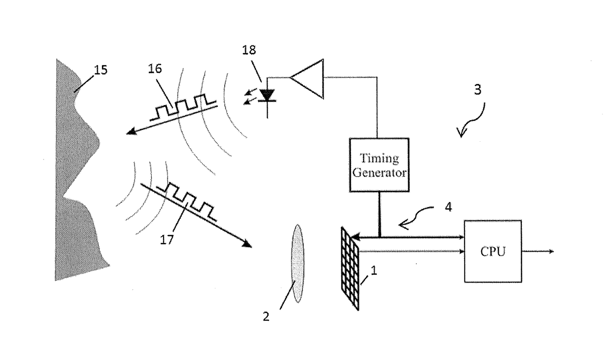
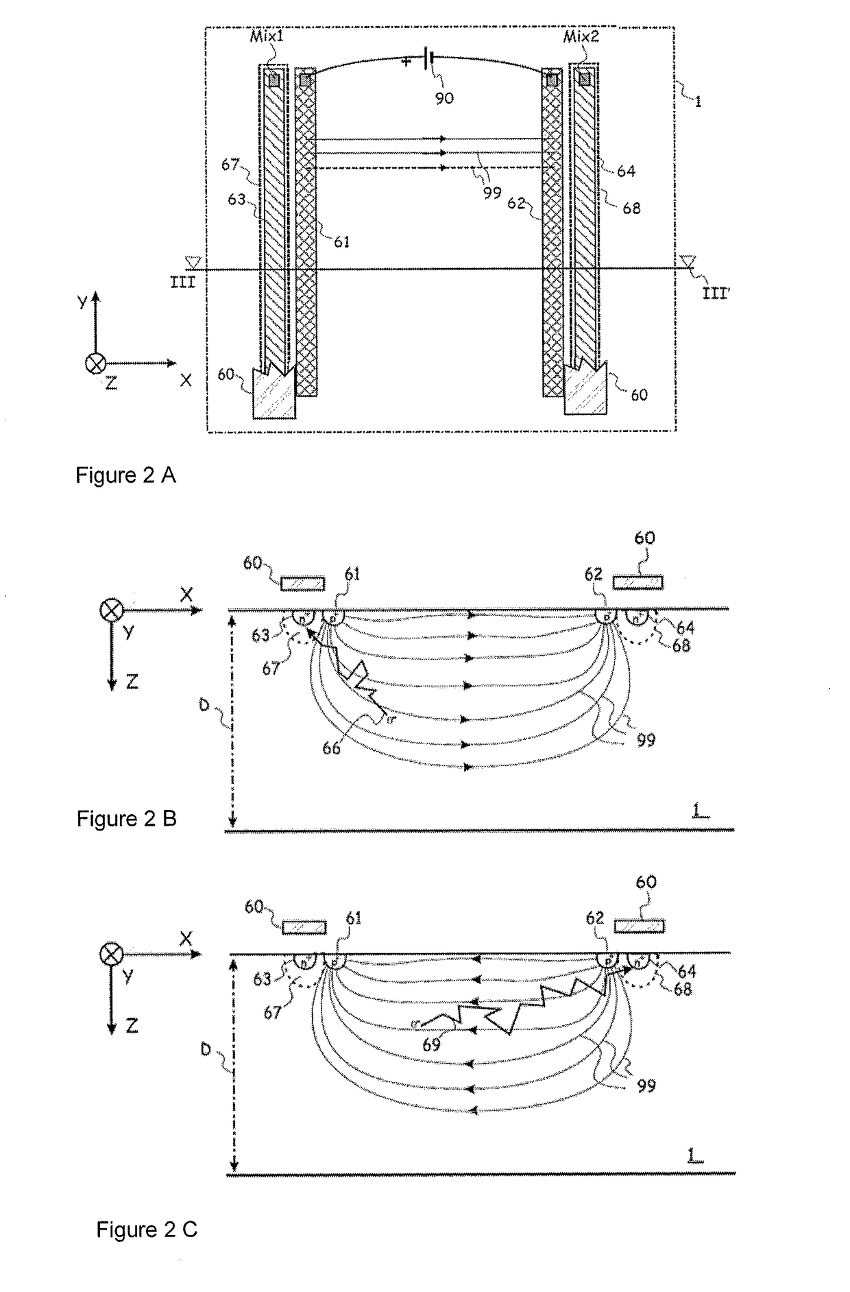
[0030]The invention will be explained with reference to p-type epitaxial layer and substrate, but the present invention includes within its scope a complementary device whereby p and n regions become n and p regions respectively. A skilled person can make such modification without departing from the spirit of the invention.

[0031]It should also be understood that the terms n, p, n+, p+, p− and p−−, n-well, p-well, deep n-well and deep p-well are well known by the one skilled in the art. The terms n, p, n+, p+, p− and p−− refer to ranges of doping levels in semiconductor materials well known by the one skilled in the art.

[0032]The terms n and p refer to n-doped and p-doped regions, usually arsenic and boron doped regions, respectively. n+, p+ refer to highly doped shallow contact regions for NWELL and PWELL respectively. p− refers to lowly doped p type region such as a PWELL and p−− refers to very lowly doped p type region close to intrinsic concentration at least 2 orders of magnitud...


PUM


Abstract

The invention relates to a majority current assisted detector device, comprising a semiconductor layer of a first conductivity type epitaxially grown on a semiconductor substrate, at least two control regions of the first conductivity type, at least two detection regions of a second conductivity type opposite to the first conductivity type, and a source for generating a majority carrier current in the semiconductor layer between the two control regions, the majority current being associated with an electrical field. The detection regions surround the control regions, thereby forming at least two taps. The device is configured for backside illumination and further comprises a well of the first conductivity type between the two detection regions for insulating the detection regions. The well comprises pixel circuitry elements.

Description

TECHNICAL FIELD OF THE INVENTION[0001]The invention relates to a detector device assisted by majority current for detecting an electromagnetic radiation impinging on a semiconductor layer, wherein a majority carrier current is generated between two control regions and wherein photo-generated minority carriers are directed towards a detection region under the influence of an electrical field generated between the control regions.[0002]The invention can be used in imagers, particularly Time-Of-Flight imagers, video games and other domestic appliances, etc.BACKGROUND OF THE INVENTION[0003]Computer vision is a growing research field that includes methods for acquiring, processing, analysing, and understanding images. Notably, one theme of research in computer vision is the depth perception or, in other words, the three-dimensional (3D) vision.[0004]Time-Of-Flight technology, just to take this example, is one of the most promising technologies for depth perception. A Time-Of-Flight (TOF)...

Claims


Application Information

Patent Timeline
Patent Type & Authority Applications(United States)
IPC IPC(8): H01L27/146H01L31/11G01S7/486G01S7/4863G01S17/894
CPCH01L27/1461H01L31/11H01L27/1464G01S7/4863H01L27/14609H01L31/101G01S17/894
Inventor FOTOPOULOU, KYRIAKI KORINAVAN DER TEMPEL, WARD
Owner SOFTKINETIC SENSORS
Why Eureka
Try Eureka