Spatially Multiplexed Dielectric Metasurface Optical Elements

a dielectric metasurface and optical element technology, applied in the field of optical devices and methods, can solve the problems of inability to achieve achromatic imaging based on metasurfaces at visible wavelengths, limited use of dgmoe technology in its current state, and inability to achieve achromatic imaging based on metasurfaces, etc., to achieve the effect of improving the performance of conventional optical elements, facilitating the creation of optical elements, and high packing density

Active Publication Date: 2017-08-03
THE BOARD OF TRUSTEES OF THE LELAND STANFORD JUNIOR UNIV +2
View PDF7 Cites 50 Cited by
  • Summary
  • Abstract
  • Description
  • Claims
  • Application Information

AI Technical Summary

Benefits of technology

[0005]In one aspect, the present invention provides dielectric metasurface optical elements with spatially multiplexed phase profiles. The optical elements can improve performance of conventional optical elements and facilitate the creation of entirely new functionalities. The interleaved metasurface optical elements achieve high packing density of distinct optical elements on a surface. Such elements may be fabricated as a unique type of dielectric gradient metasurface optical element (DGMOE). The design of such an element includes selection of phase profiles of multiple desired optical elements. The selected profiles are broken up in a large number of segments. These segments are then spatially multiplexed with equal area / weight of each optical sub-element. By interleaving multiple optical element phase profiles and using the resulting profile to fabricate a DGMOE element, multifunctional wavefront shaping can be accomplished within one element, without reducing the numerical aperture of each sub-element.

Problems solved by technology

There remain certain limitations of the DGMOE technology in its current state.
For example, metasurface lenses at visible wavelengths have been developed for imaging, but their use has been limited to single wavelength applications chiefly due to the large degree of chromatic aberration in the lens design.
Although various efforts have been made to avoid this problem, achromatic imaging based on metasurfaces at visible wavelengths is still not available.

Method used


Image

  • Spatially Multiplexed Dielectric Metasurface Optical Elements
  • Spatially Multiplexed Dielectric Metasurface Optical Elements
  • Spatially Multiplexed Dielectric Metasurface Optical Elements

Examples


Embodiment Construction

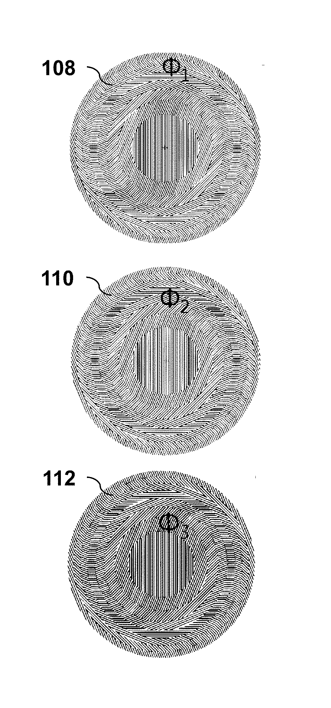
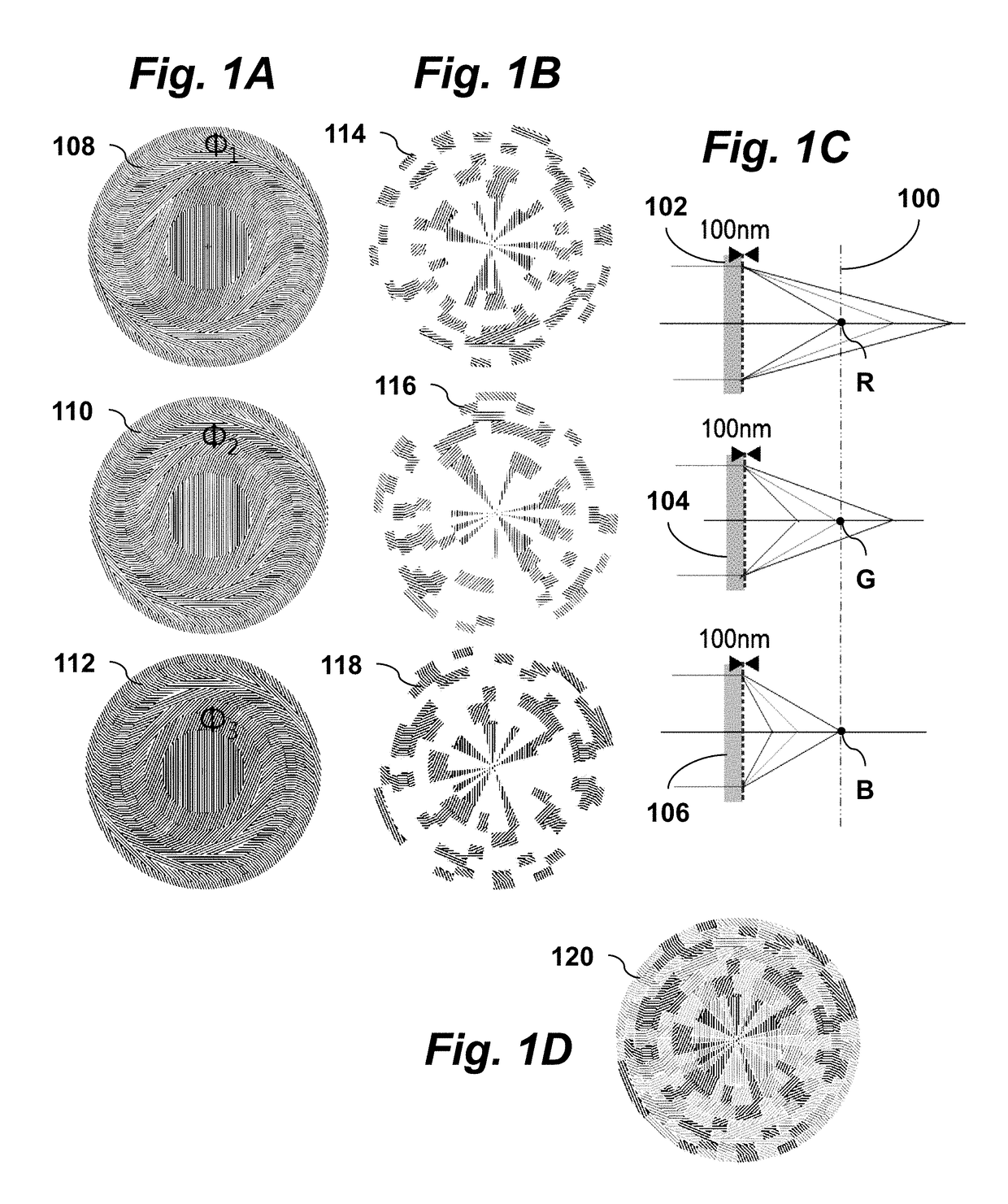
[0033]Embodiments of the present invention provide interleaved metasurface optical elements that realize multiple distinct optical functions on a single surface.

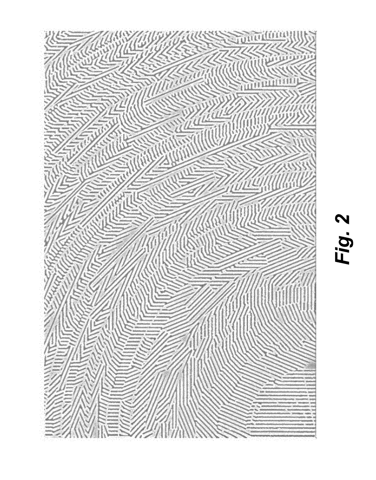
[0034]According to the principles of the invention, the phase profiles of multiple desired optical sub-elements are spatially divided into a large number of segments which are then interleaved, preferably with equal area / weight of each optical sub-element, to create spatial multiplexing of the phase profiles. By interleaving phase profiles of multiple optical sub-elements, multifunctional wavefront shaping is realized within one element, without reducing the numerical aperture of each sub-element. As examples, several specific embodiments of such multi-functional optical elements are described in detail below, including an axial multi-foci metasurface lens, lateral multi-foci metasurface lens, and polarization independent metasurface lens.

[0035]One illustrative embodiment of the invention is a metalens which can focus three ...


PUM


Abstract

A multifunctional dielectric gradient metasurface optical device has a layer of nanoscale dielectric gradient metasurface optical antenna elements deposited on a substrate layer, arranged with spatially varying orientations, shapes, or sizes in the plane of the device such that the optical device has a spatially varying optical phase response capable of optical wavefront shaping. The spatially varying optical phase response is a spatial interleaving of multiple distinct phase profiles corresponding to multiple optical sub-elements, thereby providing multifunctional wavefront shaping in the single optical element.

Description

CROSS-REFERENCE TO RELATED APPLICATIONS[0001]This application claims priority from U.S. Provisional Patent Application 62 / 288,935 filed Jan. 29, 2016, which is incorporated herein by reference.FIELD OF THE INVENTION[0002]The present invention relates generally to optical devices and methods. More specifically, it relates to integrated dielectric gradient metasurface optical elements (DGMOE).BACKGROUND OF THE INVENTION[0003]Nanophotonics has started to facilitate the replacement of bulky optical components by ultrathin, planar elements. The recent realization of metasurfaces, metamaterials of reduced dimensionality, is of particular relevance as it is opening up new opportunities to realize virtually flat optics. Metasurfaces can improve performances of conventional optical elements and facilitate the creation of entirely new functionalities, which were not explored yet. In particular, gradient metasurfaces are 2D optical elements capable of manipulating light by imparting local, spa...

Claims


Application Information

Patent Timeline
Patent Type & Authority Applications(United States)
IPC IPC(8): G02B1/00G02B5/00
CPCG02B5/008G02B1/002G02B1/00G02B5/00
Inventor LIN, DIANMINBRONGERSMA, MARK L.HASMAN, EREZKIK, PIETER G.HOLSTEEN, AARON L.
Owner THE BOARD OF TRUSTEES OF THE LELAND STANFORD JUNIOR UNIV
Why Eureka
Try Eureka