Monolithic Two-Dimensional Optical Fiber Array

a two-dimensional, optical fiber technology, applied in the direction of optics, instruments, optical light guides, etc., can solve the problems of large insertion loss errors, angular pointing errors at the output, and fiber bending some amount, so as to reduce assembly complexity and minimize component costs

Active Publication Date: 2017-08-03
II VI DELAWARE INC
View PDF8 Cites 3 Cited by
  • Summary
  • Abstract
  • Description
  • Claims
  • Application Information

AI Technical Summary

Benefits of technology

[0008]The needs remaining in the prior art are addressed by the present invention, which relates to a two-dimensional optical fiber array and a method for constructing an array in a manner that provides the necessary alignment requirements while minimizing component cost and reducing the assembly complexity, especially in higher N×N 2D fiber arrays.

Problems solved by technology

Note that the optical arrangement is typically a conjugate imaging system so that a position error of the fiber at the input will be beam position error at the output fiber.
Very small changes (i.e., on the order of a micron) create large insertion loss errors.
While shown in this case as maintaining its optical axis, insertion of optical fibers through apertures may also result in the fiber experience some amount of bending, also creating angular pointing error at the output.
Fiber and thus bean pointing error impinging onto a collimating lens produces an output beam that is displaced relative to the optical axis of the system.
To accommodate this displacement (so as to avoid clipping, scattering, and cross-talk), the MEMS micro-mirrors would need to increase in size, with the undesirable effect of reducing their density or increasing the complexity of the MEMS design.
Thus, problems associated with creating free-space optical cross-connections in high volume resides with the 2D fiber array requiring a low pitch, error, as well as a low pointing error.
The cost of fabricating multiple silicon wafers with different-sized vias, and then manipulating a stack of these wafers to align the vias is prohibitive from a cost point of view (although the required, precise alignment may be achieved).
Furthermore, it is more costly and, difficult to produce high aspect ratios as previously described.
Locating individual wafers farther from each other axially can help address pointing error issues, but increases the difficulty of assembly of such 2D arrays, and ultimately increases the cost.
Here, the assembly time is significant and cumbersome, again resulting in an expensive process.
Additionally, since each element of this configuration is a precisely made component, the final structure can be costly.

Method used


Image

  • Monolithic Two-Dimensional Optical Fiber Array
  • Monolithic Two-Dimensional Optical Fiber Array
  • Monolithic Two-Dimensional Optical Fiber Array

Examples


Embodiment Construction

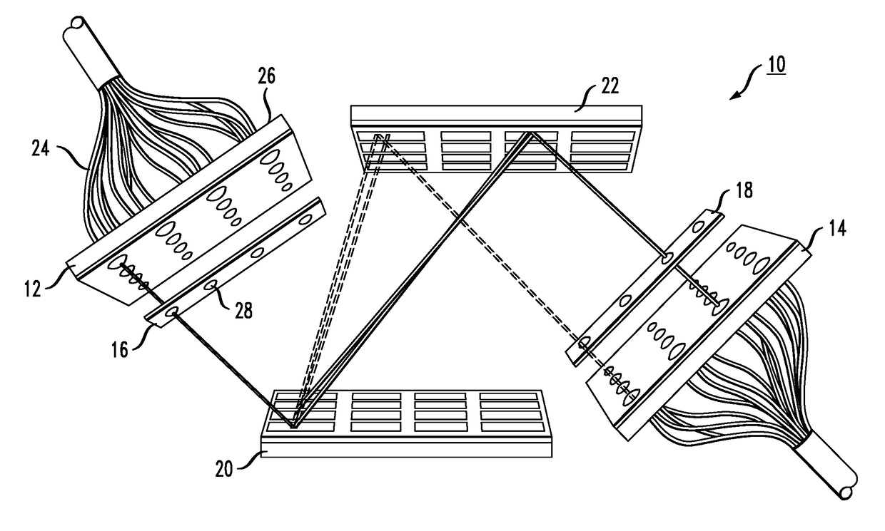
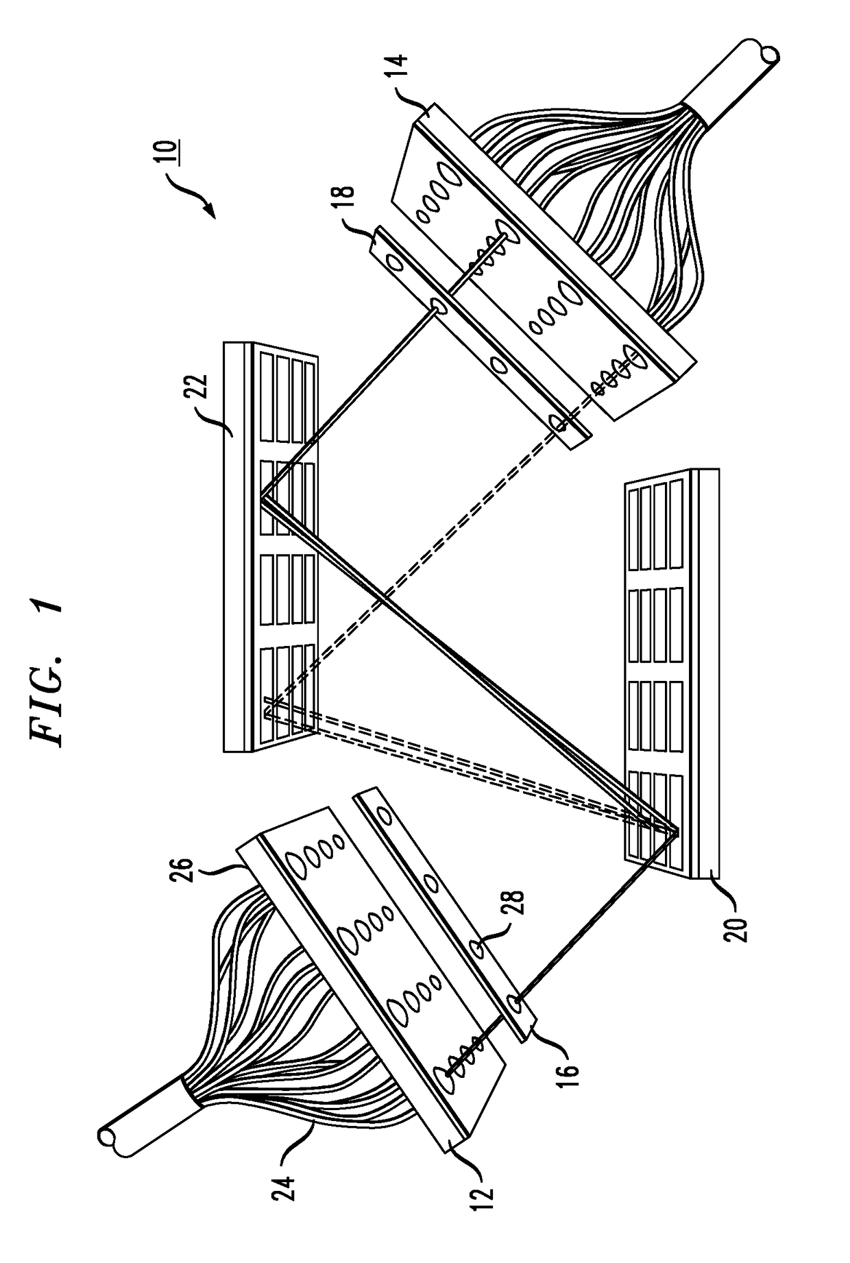
[0031]As briefly mentioned above, FIG. 1 illustrates a typical optical communication switching system 10 that may utilize the monolithic 2D fiber array component of the present invention. As shown, switching system 10 provides “fiber-to-free-space” switching between a first 2D fiber array 12 and a second 2D fiber array 14 via associated lens arrays 16,18 and MEMS arrays 20, 22. Each fiber array includes a plurality of individual optical fibers 24, separated by a predetermined spacing (hereinafter referred to as “pitch”) and coextensive with the surface of the array to direct light beams in a direction perpendicular to the array surface (pointing, as discussed above in association with FIG. 2).

[0032]Referring to first 2D fiber array 12, fibers 24 are shown as being introduced through the back side of an array substrate 26 and distributed in an array configuration (here, a 4×4 array). Array substrate 26 is formed such that the endfaces of the inserted fibers align with a set of indivi...


PUM


Abstract

A two-dimensional (2D) optical fiber array component takes the form of a (relatively inexpensive) fiber guide block that is mated with a precision output element. The guide block and output element are both formed to include a 2D array of through-holes that exhibit a predetermined pitch. The holes formed in the guide block are relatively larger than those in precision output element. A loading tool is used to hold a 1×N array of fibers in a fixed position that exhibits the desired pitch. The loaded tool (holding the pre-aligned 1×N array of fibers) is then inserted through the aligned combination of the guide block and output element, and the fiber array is bonded to the guide block. The tool is then removed, re-loaded, and the process continued until all of the 1×N fiber arrays are in place. By virtue of using a precision tool to load the fibers, the guide block does not have to be formed to exhibit precise through-hole dimensions, allowing for a relatively inexpensive guide block to be used.

Description

TECHNICAL FIELD[0001]The present invention relates to a two-dimensional optical fiber array component and a method for constructing an array component in a manner that provides the required alignment tolerances while minimizing component cost and reducing the assembly complexity.BACKGROUND[0002]Optical communication systems, particularly those associated with telecommunications and data center applications, face an ever-increasing need for larger optical switching configurations, such as optical cross-connects and “fiber-to-free-space” switching fabrics. The interconnectivity of devices via Internet-based cloud computing, as well as cloud storage capabilities, has raised the demand for lower cost optical communication systems that are able to easily and quickly switch signal paths.[0003]Optical routing of one path of an N×N array of input ports to any other output port of an N×N array of outputs will be further enabled by the development of a readily producible two-dimensional (2D) ...

Claims


Application Information

Patent Timeline
Patent Type & Authority Applications(United States)
IPC IPC(8): G02B6/36
CPCG02B6/3644G02B6/3668G02B6/3692G02B6/3672G02B6/3833G02B6/3885G02B6/3518G02B6/3556
Inventor FILIPOWICZ, MARKGARRETT, MARK H.
Owner II VI DELAWARE INC
Why Eureka
Try Eureka