Bit-cell voltage distribution system

a voltage distribution system and bit-cell technology, applied in the direction of information storage, static storage, digital storage, etc., can solve the problems of disturbed error, unstable read error at a bit-cell, etc., and achieve the effect of improving the static noise margin of the bit-cell

Active Publication Date: 2017-08-17
APPLE INC
View PDF0 Cites 1 Cited by
  • Summary
  • Abstract
  • Description
  • Claims
  • Application Information

AI Technical Summary

Benefits of technology

[0006]In various embodiments, a bit-cell voltage distribution system is disclosed where a voltage distribution circuit connects a node between a bit-cell voltage circuit and a bit-cell circuit to a word line driver circuit. The word line driver circuit may use an operating voltage to generate a word line signal as part of a read operation for the bit-cell circuit. The operating voltage may be generated by the bit-cell voltage circuit, and in some embodiments, additionally by a word line voltage circuit. As described herein, the bit-cell voltage distribution system may, at least in part, cause the bit-cell circuit to receive the operating voltage before receiving the word line signal. As a result, one or more signals of the system may be provided to the system independent of a wakeup time associated with the bit-cell circuit (because the bit-cell circuit receives the operating voltage before the word line signal). Accordingly, the bit-cell circuit may output a read value faster, as compared to a system that delays one or more control signals by a safety margin time associated with the wakeup time. Additionally, because the bit-cell receives the operating voltage before the word line signal, a static noise margin of the bit-cell may be improved, as compared to the system that delays the one or more control signals by the safety margin time.

Problems solved by technology

In some designs, bit-cells of memory devices may be subject to various forms of unstable read errors.
One form of unstable read error at a bit-cell, known as a read disturb error, occurs when a word line is connected to an operating voltage prior to a bit-cell being connected to the operating voltage.
As a result, a precharge voltage of the bit line may activate a portion of the bit-cell, destroying the data value.
Read disturb errors may be made worse by process variations, which may make signals used to connect the word line to the operating voltage propagate faster than signals used to connect the bit-cell to the operating voltage.
Additionally, a smaller retention voltage at the bit-cell may similarly make read disturb errors worse (e.g., because the bit-cell make take longer to reach a voltage where the bit line does not destroy the data value).
However, safety margins associated with such a process may, in many cases, result in additional delay.

Method used


Image

  • Bit-cell voltage distribution system
  • Bit-cell voltage distribution system
  • Bit-cell voltage distribution system

Examples


first embodiment

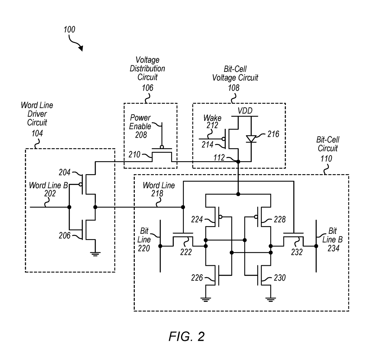
[0038]Turning now to FIG. 2, a block diagram illustrating components of bit-cell voltage distribution system 100 are shown. In the illustrated embodiment, word line driver circuit 104 includes transistor 204, and transistor 206. Voltage distribution circuit 106 includes transistor 210. Bit-cell voltage circuit 108 includes transistor 214 and diode 216. Bit-cell circuit 110 includes bit line 220, transistors 222-232, and bit line bar 234. The illustrated embodiment does not include word line voltage circuit 102. Although a particular arrangement of circuit components is illustrated with respect to FIG. 2, as further described below with reference to FIG. 4, other functionally similar arrangements of circuits (e.g., using transmission gates instead of single transistors or only using p-channel metal-oxide-semiconductor field-effect transistors) are contemplated.

[0039]As described above, bit-cell voltage circuit 108 may output an operating voltage and may output a retention voltage. In...

second embodiment

[0046]Turning now to FIG. 3, a block diagram illustrating components of bit-cell voltage distribution system 100 are shown. In the illustrated embodiment, word line voltage circuit 102 includes transistor 304. Word line driver circuit 104 includes transistor 204, and transistor 206. Voltage distribution circuit 106 includes transistor 210. Bit-cell voltage circuit 108 includes transistor 214 and diode 216. Bit-cell circuit 110 includes bit line 220, transistors 222-232, and bit line bar 234. Although a particular arrangement of circuit components is illustrated with respect to FIG. 3, other functionally similar arrangements of circuits (e.g., using transmission gates instead of single transistors or only using p-channel metal-oxide-semiconductor field-effect transistors) are contemplated.

[0047]In the illustrated embodiment, bit-cell voltage circuit 108, word line driver circuit 104, and bit-cell circuit 110 function as described above with reference to FIG. 2. As described above, wo...

third embodiment

[0049]Turning now to FIG. 4, a block diagram illustrating components of bit-cell voltage distribution system 100 are shown. In the illustrated embodiment, word line driver circuit 104 includes transmission gate 404 and transistors 406 and 408. Voltage distribution circuit 106 includes transistor 210. Bit-cell voltage circuit 108 includes transistor 214 and diode 216. Bit-cell circuit 110 includes bit line 220, transistors 222, 226, 230, and 232, and bit line bar 234. The illustrated embodiment does not include word line voltage circuit 102.

[0050]As compared to the first embodiment of bit-cell voltage distribution system 100 illustrated with reference to FIG. 2, word line bar signal 202 and the inverter formed by transistors 204 and 206 of FIG. 2 are replaced by word line signal 402, transmission gate 404, and an inverter formed by transistors 406 and 408. In the illustrated embodiment, voltage distribution circuit 106 is directly connected to the n-channel metal-oxide-semiconductor ...


PUM


Abstract

In some embodiments, a method includes receiving, at a voltage distribution circuit, a power enable signal. In response to the power enable signal, the voltage distribution circuit may connect a word line driver circuit to a bit-cell voltage circuit such that an operating voltage is received at a bit-cell circuit before a word line signal form the word line driver circuit is received at the bit-cell circuit, where the operating voltage is provided by the bit-cell voltage circuit. The method may further include the bit-cell circuit providing the operating voltage along a bit line based on a data stored at the bit-cell circuit and based on the word line signal. In some embodiments, a static noise margin of one or more portions of the bit-cell circuit may be improved. Additionally, in some cases, a wakeup time of the bit-cell circuit may be ignored, resulting in a faster read operation.

Description

BACKGROUND[0001]Technical Field[0002]This disclosure relates generally to a bit-cell voltage distribution system.[0003]Description of the Related Art[0004]In some designs, bit-cells of memory devices may be subject to various forms of unstable read errors. One form of unstable read error at a bit-cell, known as a read disturb error, occurs when a word line is connected to an operating voltage prior to a bit-cell being connected to the operating voltage. If the word line is connected to the operating voltage prior to the bit-cell being connected to the operating voltage, a bit line may be connected to a data value of the bit-cell while the bit-cell is operating using a retention voltage. As a result, a precharge voltage of the bit line may activate a portion of the bit-cell, destroying the data value. Read disturb errors may be made worse by process variations, which may make signals used to connect the word line to the operating voltage propagate faster than signals used to connect ...

Claims


Application Information

Patent Timeline
Patent Type & Authority Applications(United States)
IPC IPC(8): G11C11/418G11C8/08
CPCG11C8/08G11C11/418
Inventor ABU-RAHMA, MOHAMED H.SINANGIL, YILDIZ
Owner APPLE INC
Why Eureka
Try Eureka