Semiconductor device and manufacturing method thereof

A manufacturing method and semiconductor technology, which are applied in the fields of semiconductor/solid-state device manufacturing, semiconductor devices, electric solid-state devices, etc., can solve the mismatch between the first channel transistor and the second channel transistor, the performance degradation of static random access memory, static noise Tolerance reduction and other issues, to achieve the effect of high operating current, low threshold voltage, and improved performance

Active Publication Date: 2020-12-04
晶芯成(北京)科技有限公司
View PDF7 Cites 2 Cited by
  • Summary
  • Abstract
  • Description
  • Claims
  • Application Information

AI Technical Summary

Problems solved by technology

[0003] The key indicator for considering the stability of 6T SRAM cells is static noise redundancy or static noise margin (SNM, Static Noise Margin), which is usually defined as the difference between the operating current of the pull-down transistor and the operating current of the pass transistor Ratio, in order to improve the static noise margin, the width of the active region in the pull-down transistor is usually designed to be larger than the width of the active region in the pass transistor, but in the actual manufacturing process, due to the limitation of lithography and etching process capabilities, the pass transistor The shape of the active region in the middle is prone to distortion, causing a mismatch between the first pass transistor and the second pass transistor, thus resulting in reduced static noise margin, resulting in reduced performance of the SRAM

Method used


Image

  • Semiconductor device and manufacturing method thereof
  • Semiconductor device and manufacturing method thereof
  • Semiconductor device and manufacturing method thereof

Examples


Embodiment Construction

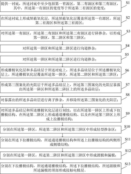
[0062] Embodiments of the present invention are described below through specific examples, and those skilled in the art can easily understand other advantages and effects of the present invention from the content disclosed in this specification. The present invention can also be implemented or applied through other different specific implementation modes, and various modifications or changes can be made to the details in this specification based on different viewpoints and applications without departing from the spirit of the present invention.

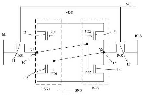
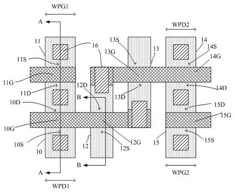
[0063] It should be noted that the diagrams provided in this embodiment are only schematically illustrating the basic idea of ​​the present invention, and only the components related to the present invention are shown in the diagrams rather than the number, shape and shape of the components in actual implementation. Dimensional drawing, the type, quantity and proportion of each component can be changed arbitrarily during actual impleme...


PUM

PropertyMeasurementUnit
thicknessaaaaaaaaaa
thicknessaaaaaaaaaa
thicknessaaaaaaaaaa

Abstract

The invention provides a semiconductor device and a manufacturing method thereof. The method comprises the steps of providing a substrate which at least comprises a first active region, a second active region and a third active region, wherein the width of the first active region is equal to the width of the second active region, forming a shielding oxide layer on the substrate, wherein the shielding oxide layer covers the first active region, the second active region and the third active region, forming a patterned photoresist layer on the shielding oxide layer, wherein the patterned photoresist layer exposes the shielding oxide layer on the first active region and the second active region, and taking the exposed shielding oxide layer as a mask, carrying out ion doping on the first activeregion and the second active region so as to form a first channel in the first active region and the second active region, and removing the patterned photoresist layer. According to the manufacturingmethod of the semiconductor device, the performance of the semiconductor device can be improved.

Description

technical field [0001] The invention relates to the technical field of semiconductors, in particular to a semiconductor device and a manufacturing method thereof. Background technique [0002] Static Random Access Memory (SRAM, Static Random Access Memory) is a very common embedded memory in Logic circuits. Due to its high-density mode, the yield rate of integrated circuits is largely limited by the performance of embedded memory. Currently, the most common SRAM cell is the 6T structure. [0003] The key indicator for considering the stability of 6T SRAM cells is static noise margin or static noise margin (SNM, Static Noise Margin), which is usually defined as the difference between the operating current of the pull-down transistor and the operating current of the pass transistor Ratio, in order to improve the static noise margin, the width of the active region in the pull-down transistor is usually designed to be larger than the width of the active region in the pass trans...

Claims


Application Information

Patent Timeline
Patent Type & Authority Applications(China)
IPC IPC(8): H01L21/8244H01L27/11
CPCH10B10/12
Inventor 陈兴
Owner 晶芯成(北京)科技有限公司
Why Eureka
Try Eureka