Optimal power collection control method and apparatus in solar photovoltaic power generation system
- Summary
- Abstract
- Description
- Claims
- Application Information
AI Technical Summary
Benefits of technology
Problems solved by technology
Method used
Image
Examples
embodiment 1
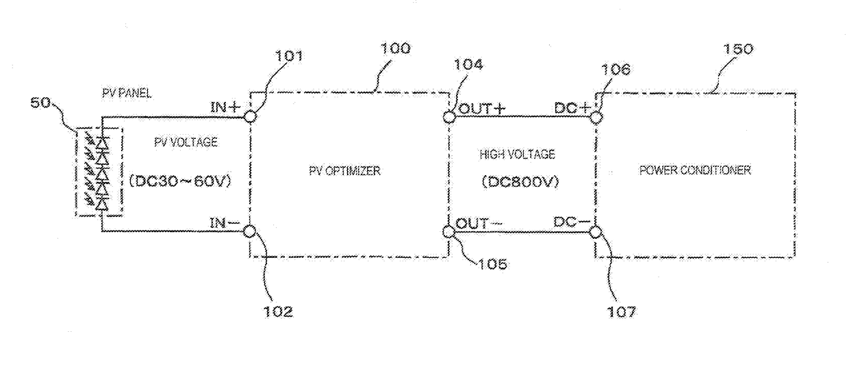
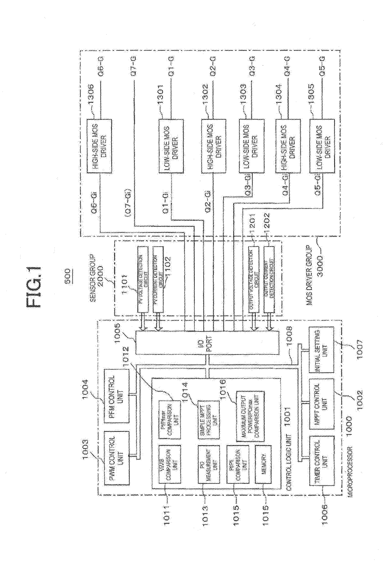
[0100]FIG. 1 is a functional block diagram for controlling an optimizer included in an optimal power collection control apparatus in a solar photovoltaic power generation system according to the present invention. This functional block diagram is for illustrating the optimal power collection control method described later with reference to FIGS. 4 and 5, and shows the configuration of a control apparatus that executes processes. This control apparatus 500 is a DC-DC converter that includes a switching regulator driven at a switching frequency (Pfi) through pulse frequency modulation control (PFM) and pulse width modulation control (PWM), and is for controlling an optimizer that steps up a DC input voltage from the solar photovoltaic panel to a predetermined DC high voltage and converts the stepped-up DC voltage into a grid connection voltage.
[0101]This control apparatus 500 includes a microprocessor 1000, a sensor group 2000, and a MOS driver group 3000. The microprocessor 1000 is c...
embodiment 2
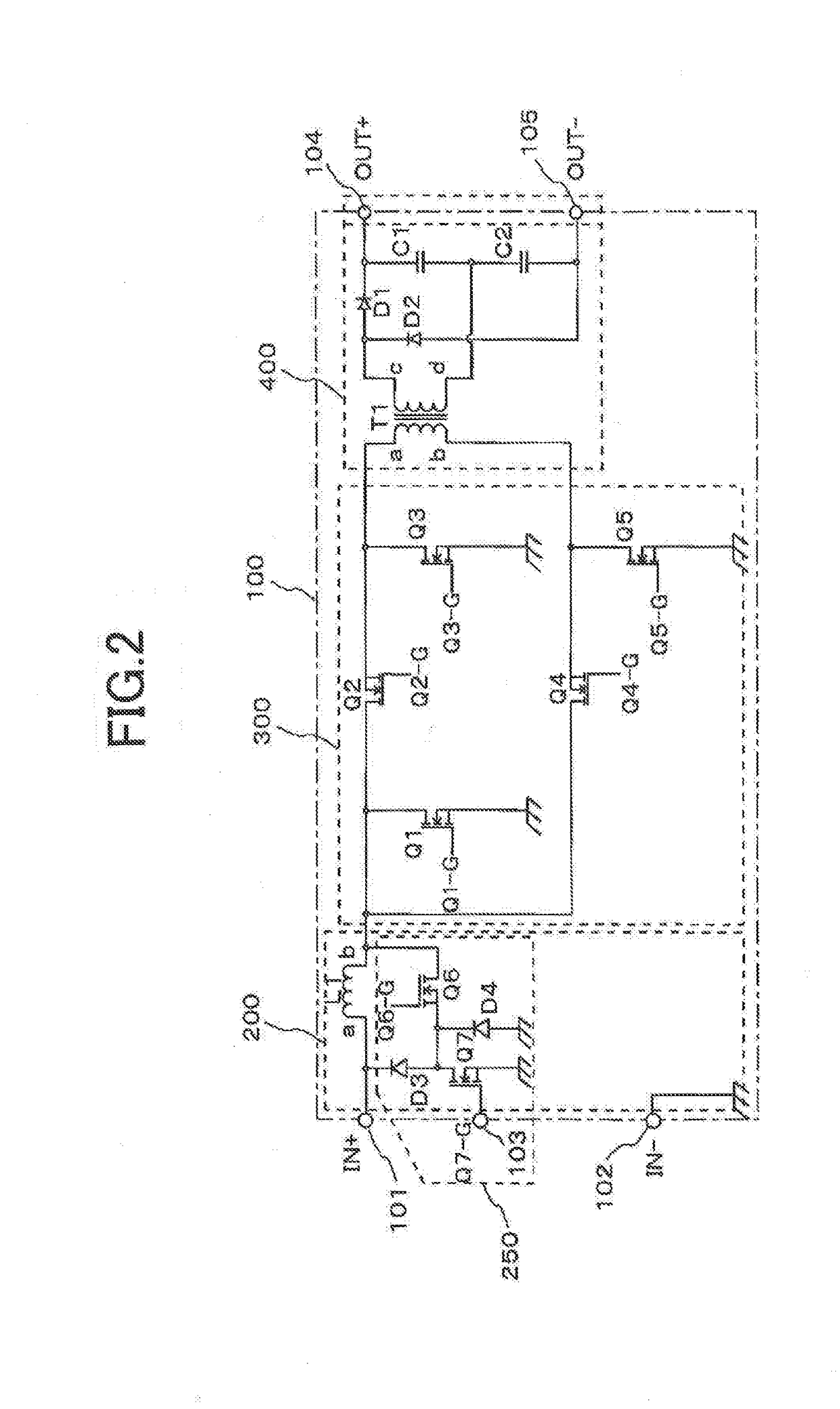
[0148]FIG. 7 is a circuit diagram for illustrating the configuration of the optimizer used for Embodiment 2 of the optimal power collection control apparatus in the solar photovoltaic power generation system according to the present invention. In the aforementioned Embodiment 1, the input means 200 is provided with the surge protection circuit that includes the sixth switching transistor Q6 and the seventh switching transistor Q7. In Embodiment 2, the surge protection circuit provided for the input means 200 is configured by removing the seventh switching transistor Q7 from the circuit shown in FIG. 2 and by including only the sixth switching transistor Q6, the third diode D3 and the fourth diode D4.
[0149]The operation of Embodiment 2 of the present invention that includes the optimizer shown in FIG. 7 is that obtained by removing the portion corresponding to the seventh switching transistor Q7 in the description of Embodiment 1. That is, the circuit is that obtained by removing the...
PUM
 Abstract
Description
Claims
Application Information


