

Laminated film and flexible electronic device
a flexible electronic device and laminate film technology, applied in the direction of chemical vapor deposition coating, metallic material coating process, synthetic resin layered products, etc., can solve the problem that the gas barrier characteristics of plastic film substrates are inferior to those of glass substrates, and achieve the effect of high adhesion
- Summary
- Abstract
- Description
- Claims
- Application Information
AI Technical Summary
Benefits of technology
Problems solved by technology
Method used
Image

Examples
example 1
[0147]Using a biaxially stretched polyethylene terephthalate film (Q65HA, manufactured by Teijin DuPont Films Japan Limited, thickness: 100 μm, both surfaces were treated to promote adhesion) as a substrate, a UV-curable acrylate monomer solution (product name: ARONIX UV-3701, manufactured by Toagosei Co., Ltd.) containing no filler was applied as an organic coating solution to one surface of the substrate by a wet coating method, followed by drying at 80° C. for 1 minute, and then, the coating layer was irradiated with UV-rays (SP-9, manufactured by USHIO INC.) at an integrated dose of 30 mJ / cm2 to form an organic layer having a thickness of 2 μm. The ratio W1 / W0 of the weight W1 of an acrylate resin component contained in the obtained organic layer to the weight W0 of the organic layer was 0.8, and the ratio W2 / W0 of the weight W2 of an organic silicon compound component contained in the organic layer to the weight W0 of the organic layer was 0. It was confirmed that the obtained ...
example 2
[0152]A substrate / organic layer film 2 and a laminated film 2 were obtained in the same manner as in Example 1 except that a UV-curable acrylate monomer solution (product name: LCH1559, manufactured by Toyo Ink Co., Ltd.) containing no filler was used as the organic coating solution. The ratio W1 / W0 of the weight W1 of an acrylate resin component contained in the obtained organic layer to the weight W0 of the organic layer was 0.6, and the ratio W2 / W0 of the weight W2 of an organic silicon compound component contained in the organic layer to the weight W0 of the organic layer was 0.
[0153]It was confirmed that the substrate / organic layer film 2 had heat resistance to a temperature of 180° C. or more by the measurement of Heat resistance evaluation 1, and it was also confirmed that the rate of reduction in modulus of elasticity was 0% by the measurement of Heat resistance evaluation 2. With regard to the obtained laminated film 2, the aforementioned adhesion measuring methods (i) and ...
example 3
[0156]A substrate / organic layer film 3 and a laminated film 3 were obtained in the same manner as in Example 1 except that a UV-curable urethane acrylate monomer solution (product name: BEAMSET 381, manufactured by Arakawa Chemical Industries Ltd.) containing no filler was used as the organic coating solution. The ratio W1 / W0 of the weight W1 of an acrylate resin component contained in the obtained organic layer to the weight W0 of the organic layer was 0.7, and the ratio W2 / W0 of the weight W2 of an organic silicon compound component contained in the organic layer to the weight W0 of the organic layer was 0. It was confirmed that the substrate / organic layer film 3 had heat resistance to a temperature of 180° C. or more by the measurement of Heat resistance evaluation 1, and it was also confirmed that the rate of reduction in modulus of elasticity was 0% by the measurement of Heat resistance evaluation 2. With regard to the obtained laminated film 3, the aforementioned adhesion meas...
PUM
| Property | Measurement | Unit |
|---|---|---|
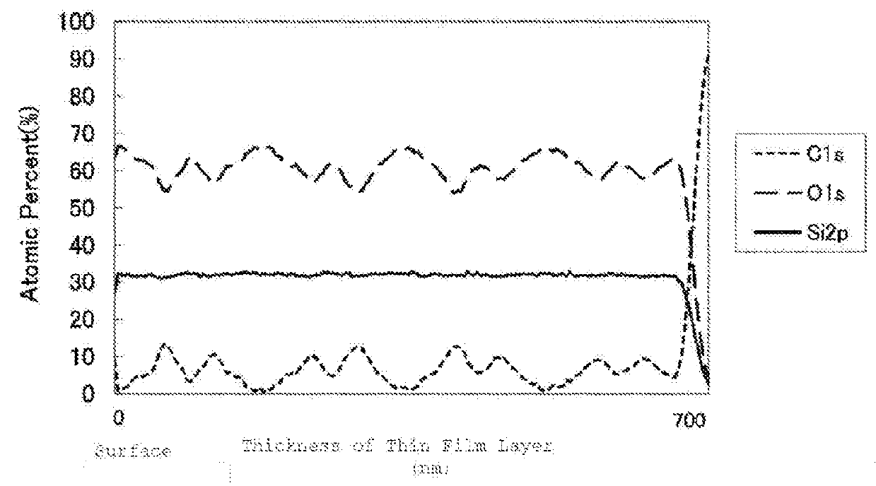
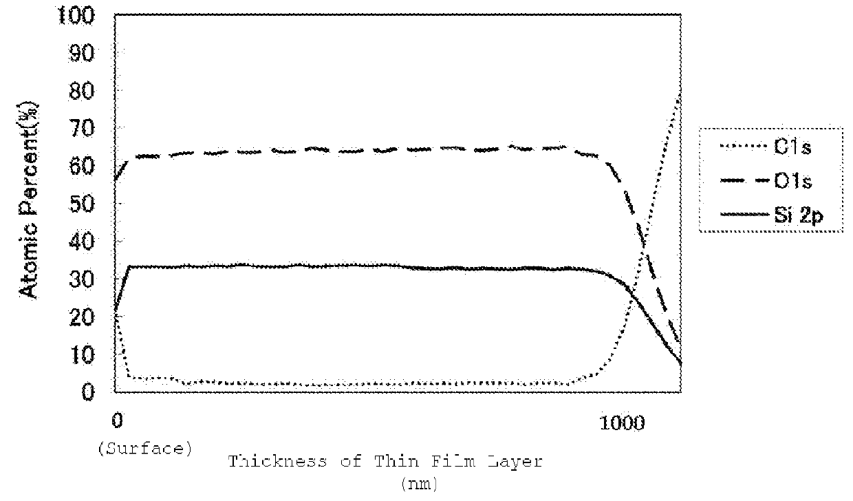
| atomic number ratio | aaaaa | aaaaa |
| glass transition temperature | aaaaa | aaaaa |
| temperature | aaaaa | aaaaa |
Abstract
Description
Claims
Application Information