Read performance of a non-volatile memory device, in particular a non-volatile memory device with buried selection transistor

a non-volatile memory and read performance technology, which is applied in the direction of solid-state devices, semiconductor devices, instruments, etc., can solve the problems of modifying the logical value of stored bits, and achieve the effects of improving the performance characteristics of non-volatile memory devices, eliminating the risk of occurrence, and reducing or even eliminating the read stress

Active Publication Date: 2017-09-28
STMICROELECTRONICS (ROUSSET) SAS
View PDF0 Cites 5 Cited by
  • Summary
  • Abstract
  • Description
  • Claims
  • Application Information

AI Technical Summary

Benefits of technology

[0009]One embodiment of the disclosure aims to improve the performance characteristics of a non-volatile memory device during a read operation, by greatly reducing, or even eliminating, the read stress so as to minimize, or even eliminate, the risk of occurrence of a ‘read disturb’ phenomenon.
[0016]It therefore becomes possible to apply a read voltage of zero to the control gate during a read operation. Indeed, with such a read voltage of zero, it is possible to differentiate the state of the memory cell, since the state transistor of a memory cell in its first state (erased cell for example) will be conducting since its threshold voltage will be lower than that of a virgin cell and it will be turned off in the presence of a memory cell in its second state (programmed cell for example) since the threshold voltage will now be positive.
[0017]So, since, in read mode, there is a voltage of zero on the control gate and hence on the charge-trapping region, there are no read stresses induced, which allows the risk of the appearance of the ‘read disturb’ phenomenon to be greatly reduced, or even eliminated.
[0022]Accordingly, in such a manner as to promote a reliable differentiation of the two erased and programmed states of the memory cell when it is read, a negative threshold voltage will be advantageously chosen for the state transistor of the memory cell in the virgin state.
[0026]Those skilled in the art will be able to adjust the energy of implantation of the dopants in order to obtain a depth of the channel compatible with a transistor of the depletion-mode type, while at the same time allowing the latter to be readily turned off where necessary.
[0036]Although it would be possible to equip these memory cells of such a device with state transistors of the depletion-mode type, the advantage gained in terms of reduction of the read stress only in fact concerns one of the two twin cells, in other words the one in the process of being read, because the other twin cell has to receive a non-zero read inhibit voltage on the control gate of its state transistor so as to avoid it being simultaneously read.

Problems solved by technology

However, when such a read voltage is applied to the control gate of the state transistor, the electric field in the floating gate is modified resulting in a stress, which ‘read stress’ may lead to a ‘read disturb’ phenomenon that can result in a modification of the logical value of the stored bit.

Method used


Image

  • Read performance of a non-volatile memory device, in particular a non-volatile memory device with buried selection transistor
  • Read performance of a non-volatile memory device, in particular a non-volatile memory device with buried selection transistor
  • Read performance of a non-volatile memory device, in particular a non-volatile memory device with buried selection transistor

Examples


Embodiment Construction

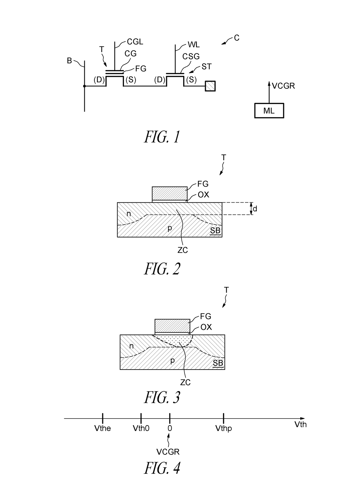
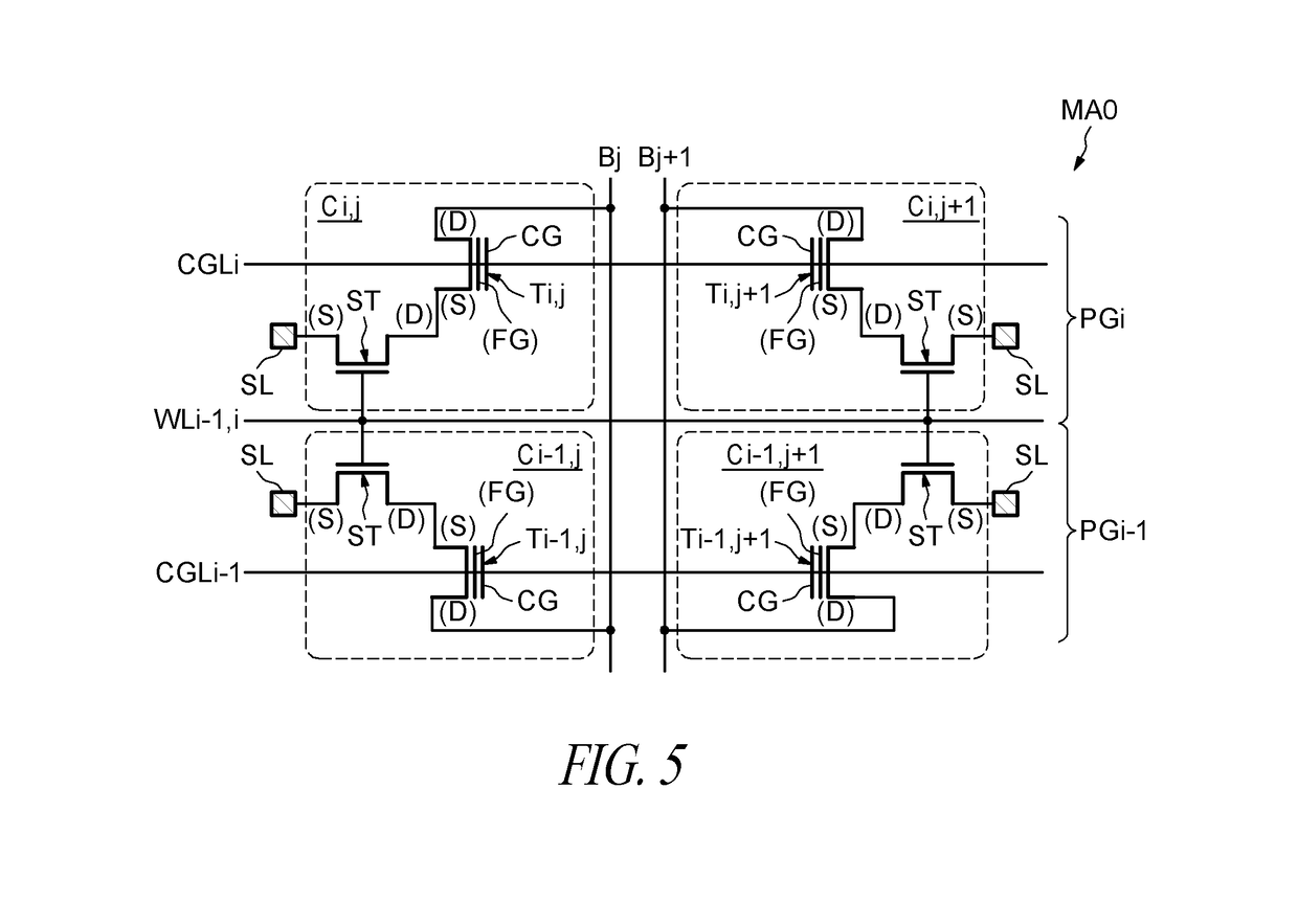
[0052]In FIG. 1, the reference C denotes a non-volatile memory cell, for example of the EEPROM type or else of the type with a buried vertical selection transistor.

[0053]More precisely, the memory cell C comprises a state transistor T comprising a floating gate FG on top of which is a control gate CG connected to a gate control line CGL. As is well known, the floating gate FG acts as a charge-trapping region that does not trap charge in a first logic state and traps charges in a second logic state.

[0054]The drain D of the state transistor T is connected to a bit line B, whereas the source of the state transistor T is connected to the drain of a selection transistor ST.

[0055]The selection transistor ST comprises a gate CSG connected to a word line WL.

[0056]The source S of the selection transistor ST is connected to a source line SL.

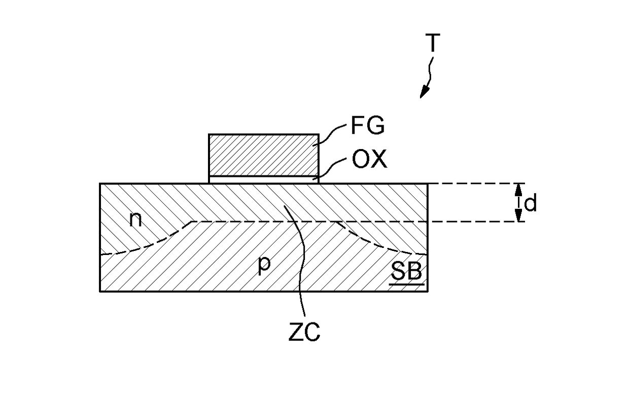
[0057]As illustrated in FIG. 2, the state transistor T is a depletion-mode transistor comprising an implanted channel ZC.

[0058]In the example illustrated ...


PUM


Abstract

The non-volatile memory device comprises memory cells each comprising a selectable state transistor having a floating gate and a control gate. The state transistor is of the depletion-mode type and is advantageously configured so as to have a threshold voltage that is preferably negative when the memory cell is in a virgin state. When the memory cell is read, a read voltage of zero may then be applied to the control gate and also to the control gates of the state transistors of all the memory cells of the memory device.

Description

BACKGROUND[0001]Technical Field[0002]Various embodiments of the disclosure and their implementation relate to non-volatile memory devices, notably those comprising buried selection transistors and, more particularly, the improvement of the read performance of such devices by reducing, or even eliminating, the stress induced in the floating gate of the state transistor of a memory cell during an operation for reading this memory cell.[0003]Description of the Related Art[0004]A non-volatile memory cell, whether it is of the electrically erasable and programmable (EEPROM) type or else of the type with vertical selection transistor, comprises a state transistor with a floating gate selectable by means of a selection transistor connected in series with the state transistor.[0005]The logical value of a bit stored in such a memory cell is represented by the value of the threshold voltage of the floating gate transistor.[0006]The programming or the erasing of a floating gate transistor cons...

Claims


Application Information

Patent Timeline
Patent Type & Authority Applications(United States)
IPC IPC(8): G11C16/34G11C16/26H01L29/788G11C16/08H01L27/115H01L29/792G11C16/04G11C16/10
CPCG11C16/3427G11C16/0466G11C16/26G11C16/10G11C16/08H01L29/7889H01L27/11582H01L27/1157H01L27/11524H01L29/792H01L29/788H01L27/11556G11C16/0433H01L28/00H10B41/27H10B41/35H10B43/27H10B43/35
Inventor LA ROSA, FRANCESCONIEL, STEPHANREGNIER, ARNAUD
Owner STMICROELECTRONICS (ROUSSET) SAS
Why Eureka
Try Eureka