Electrical conductive vias in a semiconductor substrate and a corresponding manufacturing method

a manufacturing method and semiconductor technology, applied in the direction of semiconductor/solid-state device manufacturing, electric apparatus, solid-state devices, etc., can solve the problems of affecting the production efficiency of the via, the conductive material of the via is also significant, and the application field is severely limited by the approach “via-, etc., to achieve the effect of increasing flexibility and low cos

Active Publication Date: 2017-10-12
X FAB SEMICON FOUNDRIES
View PDF7 Cites 2 Cited by
  • Summary
  • Abstract
  • Description
  • Claims
  • Application Information

AI Technical Summary

Benefits of technology

[0019]It is an object of the (claimed) invention to produce or create an electrical via at low cost and with increased flexibility in terms of the micro-technical semiconductor structures to be interconnected by the via.

Problems solved by technology

Already existing process policies for producing the vias are often already specialized too much to enable a modular flexible application.
For example, the application field is severely limited by the approach “via-first” or “via-middle”, since the contamination of standard semiconductor processes is highly problematic when using metals, such as copper, as an example.
Significant problems also arise with respect to the conductive material of the via.
Copper, which is used most often for this purpose, leads to an excessive difference in the temperature coefficient as compared to the semiconductor substrate, and it also diffuses into the adjacent material structures until a copper saturation is achieved therein, unless corresponding protective intermediate layers are provided.
These properties of copper and also the plastic-elastic properties thereof can lead to considerable problems regarding material separation and adhesion, and / or also contribute to mechanical stress in the various material layers.
Furthermore, the effect of the surrounding atmosphere on copper layers is typically associated with a temperature-dependent oxidation of this layer which is to the disadvantage of conductivity.
The deposition of layers in vertical vias for greater aspect ratios can also be realized with great difficulty only, especially when a relatively complex layer structure, as in copper, is required.
Especially in the case of great aspect ratios, common methods for layer deposition reach their limits in terms of the deposition rates to be achieved and the expenditure of time required as a result, which limits are incompatible with the usual standards for mass production.
Substantial costs are incurred with respect to the material when especially copper or tungsten are used as conductive materials for a via.

Method used


Image

  • Electrical conductive vias in a semiconductor substrate and a corresponding manufacturing method
  • Electrical conductive vias in a semiconductor substrate and a corresponding manufacturing method
  • Electrical conductive vias in a semiconductor substrate and a corresponding manufacturing method

Examples


Embodiment Construction

[0063]These—and further—embodiments will be described in detail. Initially we alternately refer to FIG. 1 and FIG. 2.

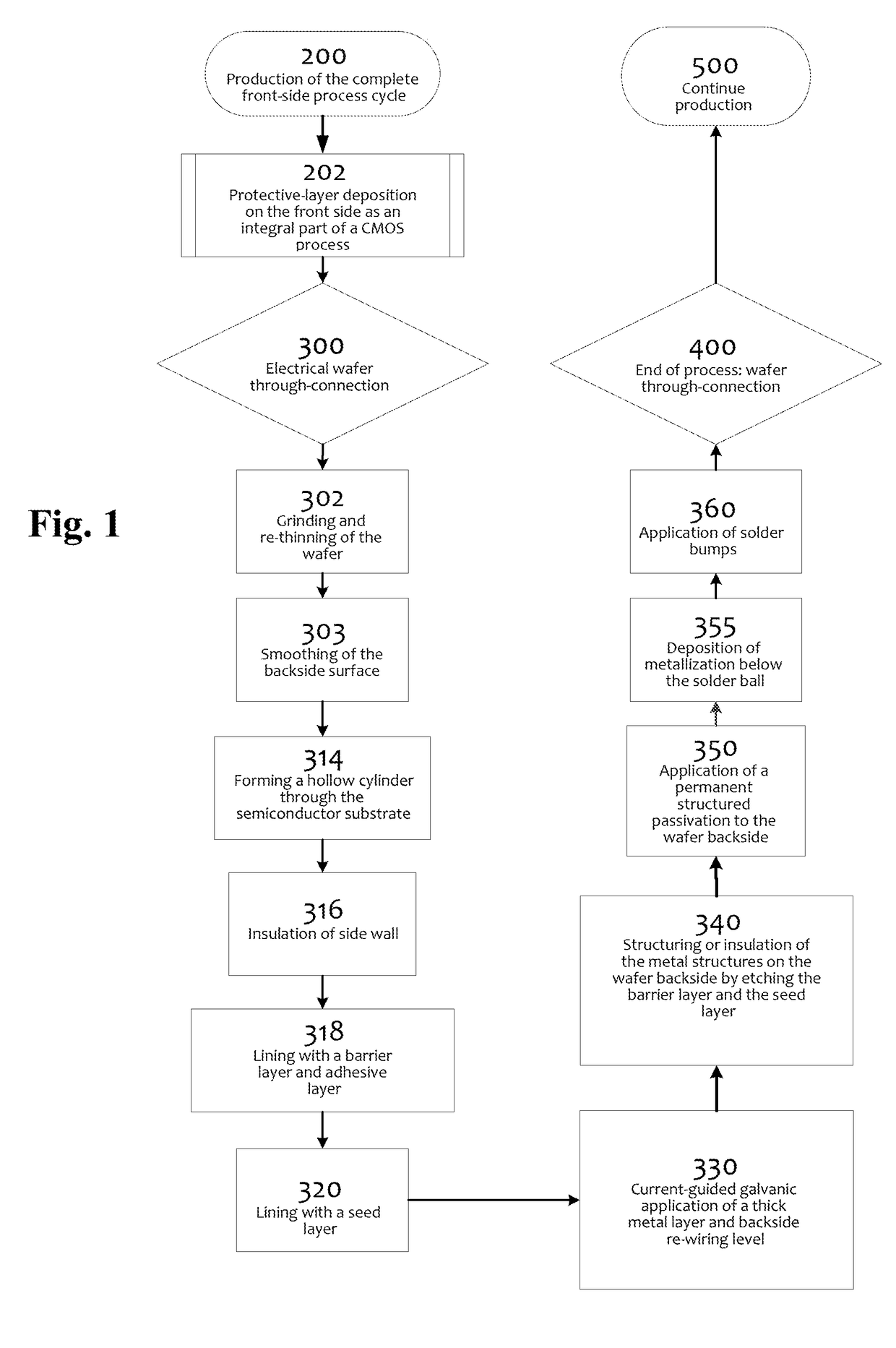
[0064]FIG. 1 schematically shows an exemplary process flow for producing a component structure including a subsequent production of an electrical via. As shown, a complete front-side process cycle 200 is initially performed, in which the desired component structure, for example, a CMOS structure, a MEMS structure is produced in combination with electronic components, etc. For this purpose, the process technologies required for this are employed, as described above, without having to consider the subsequent production of the via(s).

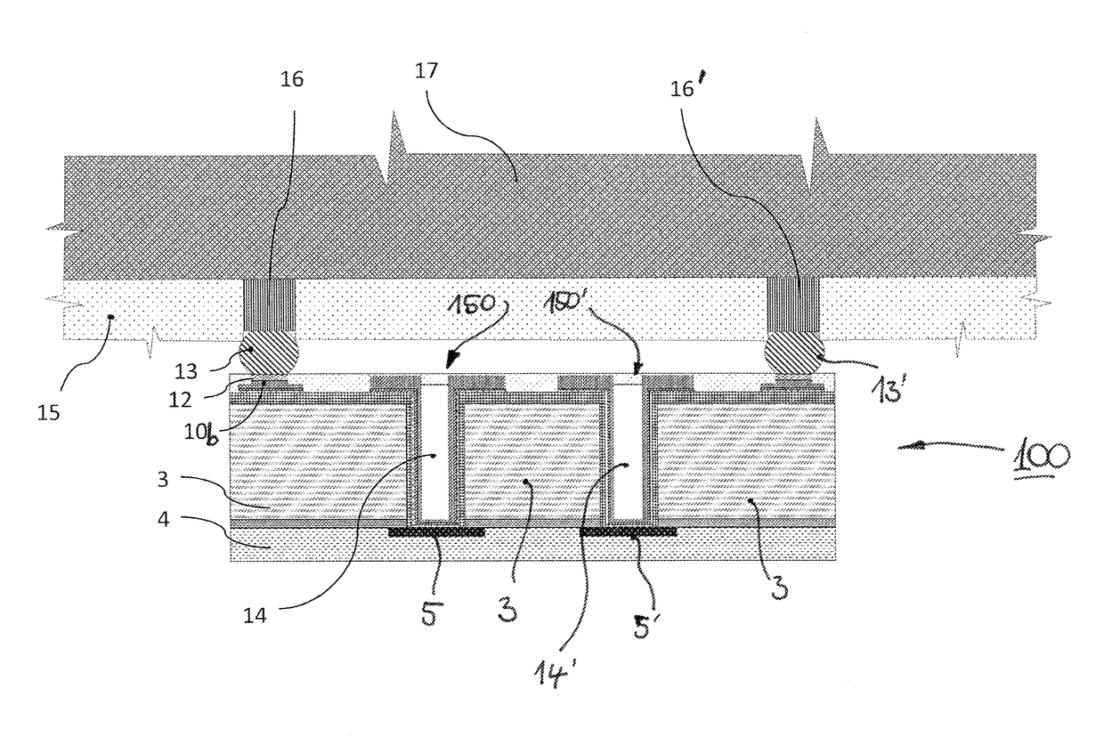
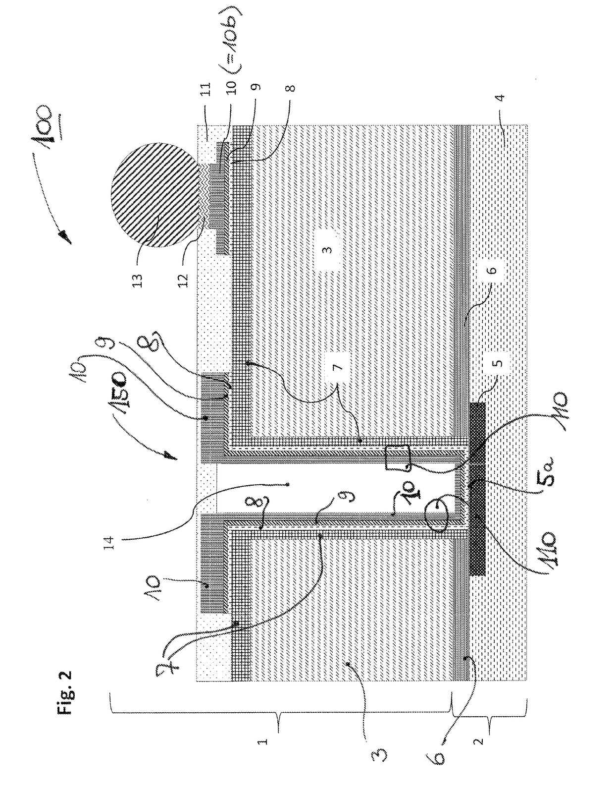
[0065]FIG. 2 shows a cross-sectional view of a component 100 in this regard, which component is referred to as a micro-technical component in order to thus describe that at least some sizes of structural elements, e.g. semiconductor devices or the like, include dimensions of 10 μm or less. The term “micro-technical” component thus includes a...


PUM


Abstract

A method is provided for producing at least one electrical via in a substrate, the method comprising: producing a protective layer over a component structure which has been produced or is present on a front side of the substrate; forming at least one contact hole which extends from a surface of a backside of the substrate to a contact surface of the component structure; forming a metal-containing and thus conductive lining in the at least one contact hole creating a hollow electrically conductive structure in the at least one contact hole; and applying a passivation layer over the backside of the substrate, the passivation layer spanning over the hollow electrically conductive structure for forming the at least one electrical via. Also provided is a micro-technical component comprising at least one electrical via.

Description

FIELD OF THE INVENTION[0001]This disclosure relates generally to the field of production of micro-technical components, e.g. microelectronic, micro-optical, micromechanical component structures, which are produced in and on a substrate and require a via through the substrate for the further interconnection of the component structure.BACKGROUND OF THE INVENTION[0002]In microelectronics and microsystems technology, apart from reducing the lateral dimensions, i.e. the dimensions in the area of a suitable substrate, e.g. a semiconductor wafer, there is an increasing tendency to also create an interconnection in the dimension perpendicular to the substrates in order to enable an overall three-dimensional integration. Especially the integration of micromechanical systems in combination with CMOS technology plays a central role in this development. Electrical vertical vias are important components for electrically interconnecting component structures, e.g. microelectromechanical structures...

Claims


Application Information

Patent Timeline
Patent Type & Authority Applications(United States)
IPC IPC(8): H01L21/768H01L23/48H01L23/00
CPCH01L21/76898H01L23/481H01L24/11H01L21/76876H01L24/03H01L24/05H01L24/13H01L2224/0235H01L2224/02372H01L2224/0347H01L2224/0401H01L2224/05008H01L2224/05022H01L2224/05147H01L2224/05155H01L2224/05186H01L2224/05567H01L2224/05644H01L2224/11H01L2224/13023H01L2224/131H01L2224/16237H01L2224/81399H01L2224/81815H01L2924/00014H01L2924/013H01L2924/04941H01L2924/014
Inventor KNECHTEL, ROYDEMPWOLF, SOPHIAGUENTHER, DANIELASCHWARZ, UWE
Owner X FAB SEMICON FOUNDRIES
Why Eureka
Try Eureka