
Eureka
For R&D, Eureka makes reading and utilizing patents & technical documents easy.
Eureka AIR
Designed for self-driven R&D workflows. Generate viable solutions, solve complex R&D challenges, empower your innovation with AI.

Eureka Materials
Designed for material experts only. Revolutionize your material R&D, from search, analyze, to developing new materials.

TechResearch
Generate reliable direction feasibility study reports for your R&D in just a few steps.

TechSeek
Discover and master advanced knowledge NOW. Basics, ideas, possibilities, all at once.

TechMind
As an expert in R&D Theories, TechMind can generates customized viable solutions instantly.

TechRisk
Analyze your overall solution with one click, know your potential R&D risks in advance.

TechMonitor
Get weekly tech updates, stay abreast of the latest tech innovations and key insights.
Super-junction semiconductor device
- Summary
- Abstract
- Description
- Claims
- Application Information
AI Technical Summary
Benefits of technology
Problems solved by technology
Method used
Image

Examples
Embodiment Construction
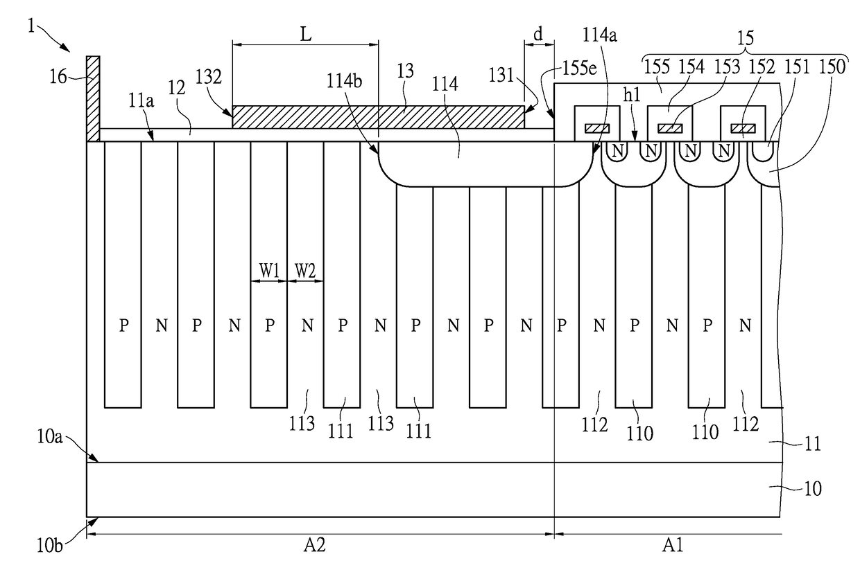
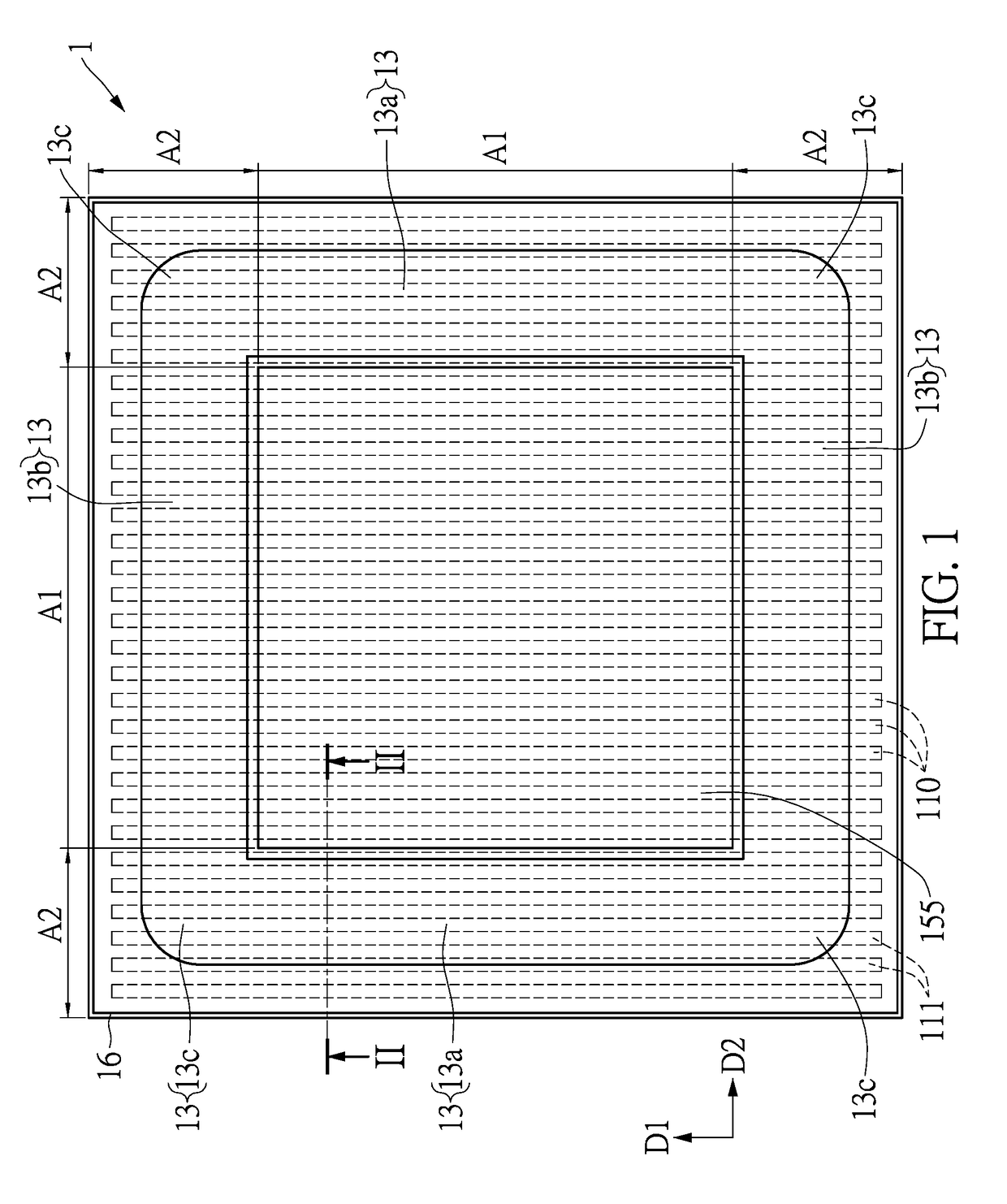
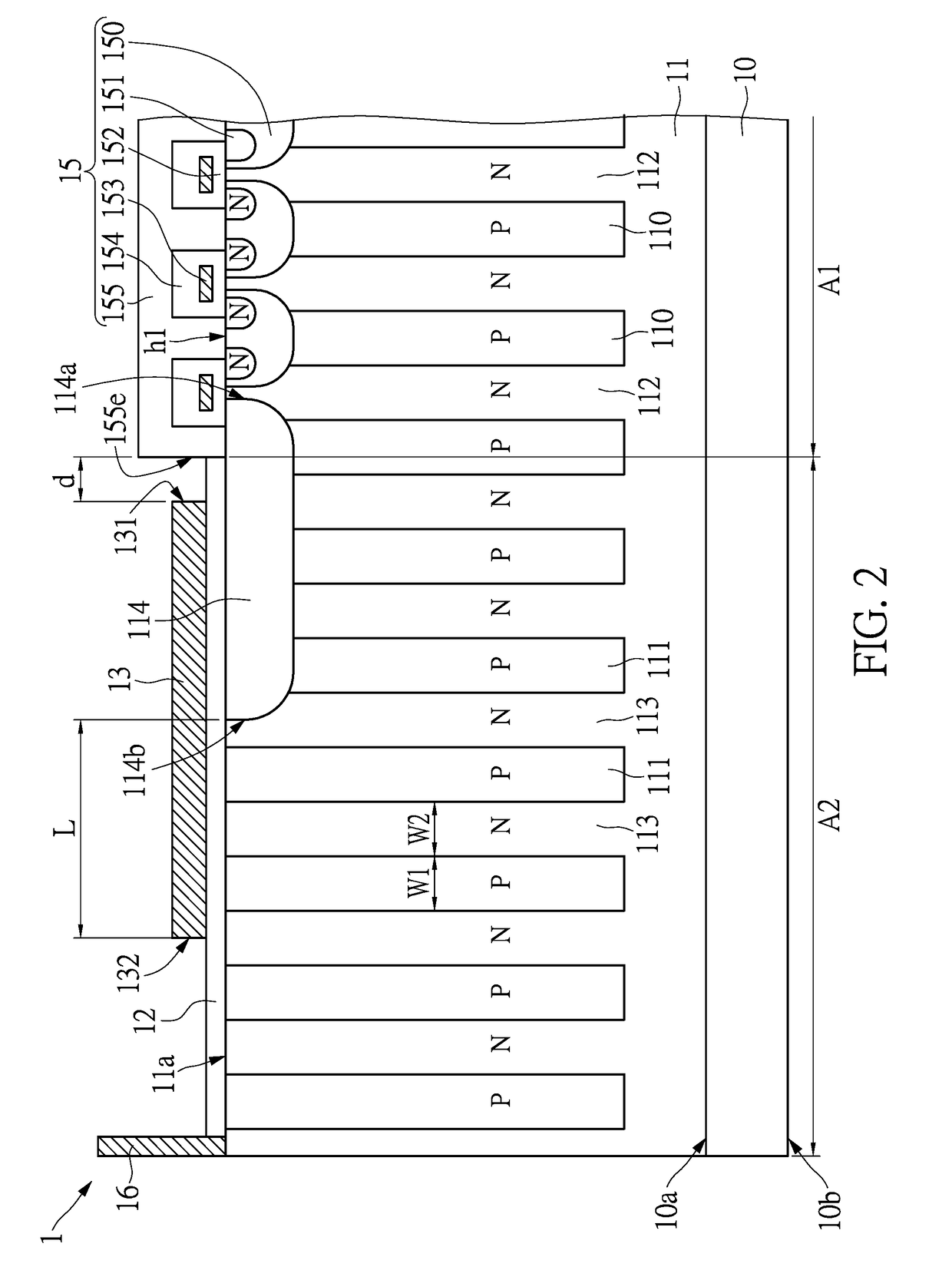
[0016]Please refer to FIG. 1 and FIG. 2. FIG. 1 shows a top view of a super junction semiconductor device according to an embodiment of the instant disclosure, and FIG. 2 shows a cross-sectional view taken on a line II-II of FIG. 1.
[0017]The super-junction semiconductor device 1 includes a substrate 10, a drift layer 11, a lightly-doped region 114, an insulating layer 12, a main loop-shaped field plate 13, and at least one transistor structure 15.
[0018]As shown in FIG. 2, the substrate 10 is made of a semiconductor and has an upper surface 10a and a back surface 10b opposite to the upper surface 10a. The substrate 10 is heavily doped with first conductivity type impurities which are distributed in a local region or throughout the substrate 10 to form a drain contact layer. In the instant embodiment, the first conductivity type impurities are distributed throughout the substrate 10, which is only used as an example, but not so as to limit the scope of the invention. A drain contact p...
PUM
 Abstract
Description
Claims
Application Information
 - R&D Engineer
- R&D Manager
- IP Professional
- Industry Leading Data Capabilities
- Powerful AI technology
- Patent DNA Extraction
Browse by: Latest US Patents, China's latest patents, Technical Efficacy Thesaurus, Application Domain, Technology Topic, Popular Technical Reports.
© 2024 PatSnap. All rights reserved.Legal|Privacy policy|Modern Slavery Act Transparency Statement|Sitemap|About US| Contact US: help@patsnap.com