Eureka AIR delivers breakthrough ideas for toughest innovation challenges, trusted by R&D personnel around the world.

Method for fine line manufacturing

Active Publication Date: 2017-11-23
ATOTECH DEUT GMBH
View PDF3 Cites 10 Cited by
  • Summary
  • Abstract
  • Description
  • Claims
  • Application Information

AI Technical Summary

Benefits of technology

The present invention provides a method for manufacturing fine line circuitry on transparent substrates using metal or metal alloy deposits. The advantages include the ability to reliably achieve line and space densities of 0.5 to 10 μm and the use of a selective deposition method that does not damage the minute structures formed in the manufacturing process. The invention also avoids over-plating, which reduces metal waste and simplifies the manufacturing process. Additionally, the metal or metal alloy structures formed in the process are uniform in height, which benefits current distribution within the device.

Problems solved by technology

Other methods such as gas phase deposition methods or electrolytic plating unselectively deposit metal on the surface which requires steps to remove the metal or metal alloy from the undesired areas.
Blade applications such as those disclosed in WO 2014 / 104846 A1 are not suitable to fill the minute structures formed in steps (i) to (v) because a force has to be applied in said case resulting in a damaging of those structures.

Method used


Image

  • Method for fine line manufacturing
  • Method for fine line manufacturing
  • Method for fine line manufacturing

Examples


Embodiment Construction

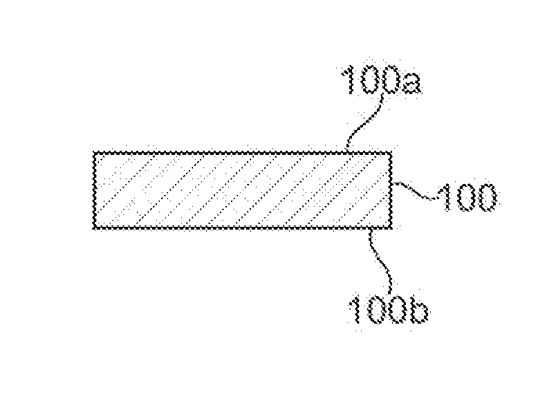
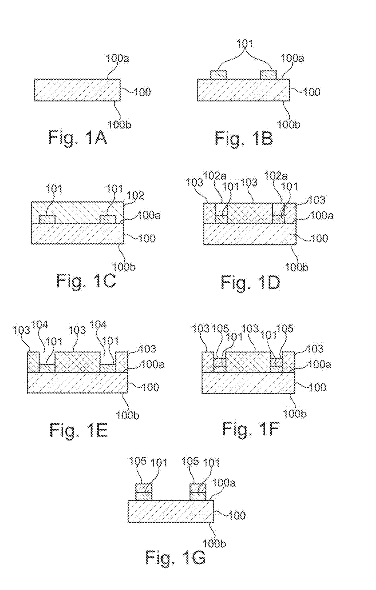
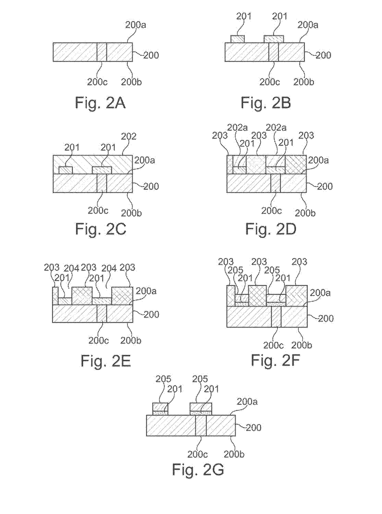
[0027]In the first step (i) of the process according to the invention as shown inFIG. 1A, a substrate (100) is provided. This substrate has a front side (100a) and a back side (100b) which are located opposite to each other. Preferably, the front side (100a) and the back side (100b) are parallel to each other. Substrates to be used in the process according to the present invention are transparent substrates. Transparency in the context of the present invention is to be understood that electromagnetic radiation used in step (iv) to photo-cure the photosensitive composition which is located on the front side (100a) of the substrate (100) can substantially transmit the substrate (100). Substantial transmission is preferably to be understood that 80% of the electromagnetic radiation can pass through the transparent substrate, i.e. the electromagnetic radiation is neither absorbed nor reflected by the transparent substrate (100). If the substrate only allows for a lower transmission of t...


PUM

PropertyMeasurementUnit
Lengthaaaaaaaaaa
Thicknessaaaaaaaaaa
Widthaaaaaaaaaa

Abstract

A novel method for the manufacturing of fine line circuitry on a transparent substrates is provided, the method comprises the following steps in the given order providing a transparent substrate, depositing a pattern of light-shielding activation layer on at least a portion of the front side of said substrate, placing a photosensitive composition on the front side of the substrate and on the pattern of light-shielding activation layer, photo-curing the photosensitive composition from the back side of the substrate with a source of electromagnetic radiation, removing any uncured remnants of the photosensitive composition; and thereby exposing recessed structures and deposition of at least one metal into the thus formed recessed structures whereby a transparent substrate with fine line circuitry thereon is formed. The method allows for very uniform and fine line circuitry with a line and space dimension of 0.5 to 10 μm.

Description

FIELD OF THE INVENTION[0001]The invention relates to a process for the manufacturing of fine line circuitry. The process is suitable for the manufacture of printed circuit boards, IC substrates, high density interconnects and advanced package substrates and the like on transparent substrates.BACKGROUND OF THE INVENTION[0002]The ongoing miniaturization of electronic devices requires sophisticated processes which allow for better line and space density (L / S) without adding significantly to the cost of the thus obtained devices. Line width and inter line distance of 10 μm (10 μm line and space—L / S) or less are currently difficult to achieve with high yield in high volume manufacturing, while sub-micron dimensions are commonplace when silicon processing methods are adopted.[0003]Generally, fine line circuitry is produced by the so-called Semi-Additive Process (SAP). This process consists of providing a substrate with a layer of copper on its (entire) surface. Then, a dry film resist is ...

Claims


Application Information

Patent Timeline
IPC IPC(8): G03F7/20H01L23/15G03F7/09G03F7/095G03F7/11H01L21/288H01L21/285H05K3/18H01L21/48C23C18/16C23C18/20C23C18/28C23C18/30C23C18/40
CPCG03F7/203C23C18/40G03F7/091G03F7/094G03F7/095G03F7/11H01L21/4846H01L23/15H05K3/181H01L21/285H01L21/288C23C18/1605C23C18/2086C23C18/285C23C18/30G03F7/2008G03F7/2002G03F7/2022C23C18/1893H05K3/0082H05K3/184H05K2201/0108H05K2203/0709H05K2203/1407
Inventor BARON, DAVID THOMASLAMPRECHT, SVEN
Owner ATOTECH DEUT GMBH
Why Eureka
Eureka Blog
Learn More