Process of forming a photoactive layer of a perovskite photoactive device

a technology of photoactive device and perovskite, which is applied in the manufacture of electrolytic capacitors, light-sensitive devices, electrolytic capacitors, etc., can solve the problems of difficult formation of continuous film on a substrate, inability to use spin coating on a larger scale, and film is susceptible to dewetting, so as to improve the processability of photoactive layer and facilitate the removal of polymer. , the effect of effective retardation

Active Publication Date: 2017-11-23
COMMONWEALTH SCI & IND RES ORG
View PDF0 Cites 27 Cited by
  • Summary
  • Abstract
  • Description
  • Claims
  • Application Information

AI Technical Summary

Benefits of technology

[0014]Due to the volatile nature of AX, equivalent or excess amount of AX compared to MX2 have been widely used when forming a perovskite layer using a perovskite precursor solution (single step) or precursor solutions (sequential deposition process). Thus despite conventional wisdom of using equivalent or excess amount of AX compared to MX2, the inventors have surprisingly discovered that the addition of a less than stoichiometric amount (i.e. greater than 0 but less than 1) of AX to MX2 in the first precursor solution applied to the substrate interferes with the crystallization of the perovskite layer in the sequential deposition process. Whilst a number of additives have been previously mixed with MX2 in an attempt to control crystallisation, the use of AX in the first precursor solution advantageously does not contaminate the perovskite composition, as this additive is a reactant added in the second step. The AX from the first precursor solution is incorporated into the final perovskite layer AMX3. No prior process has used a precursor solution having a lower than 1 molar ratio of AX in MX2, and more particularly to provide the advantage of interfering with the crystallization of the perovskite layer in the sequential deposition process.
[0111]As noted previously, the long chain structure of a polymer chain is able to effectively interfere with crystal formation of the perovskite structure. Accordingly, the addition of very small amount of a suitable polymer additive can dramatically improve the processability of perovskite solution. In some embodiments, the polymer additive comprises from 0.01 to 20 wt % of perovskite precursor. However, the polymer addition can preferably comprise from 0.05 to 18 wt % of perovskite precursor, more preferably from 0.05 to 15 wt %, yet more preferably from 0.1 to 10 wt %, even more preferably from 0.1 to 5 wt %, yet more preferably from 0.1 to 2 wt % of perovskite precursor. In one embodiment, the polymer additive comprises about 1.5 wt % of perovskite precursor.

Problems solved by technology

This crystal structure is formed rapidly in normal drying processes, and therefore can be difficult to form as a continuous film on a substrate.
However, it is not possible to use spin coating on a larger scale.
In wet coating, the wet film is susceptible to dewetting, non-homogenous crystal formation and / or the formation of pinholes, all of which have undesirable effects on the function of the photoactive layer.
These problems become increasingly more serious the greater the amount and area to which the crystalline material is applied.
Resultingly, it is more challenging to form defect free perovskite layers on a given substrate.

Method used


Image

  • Process of forming a photoactive layer of a perovskite photoactive device
  • Process of forming a photoactive layer of a perovskite photoactive device
  • Process of forming a photoactive layer of a perovskite photoactive device

Examples


example 2

e Formation Reaction Speed

Photoactive Layer Fabrication:

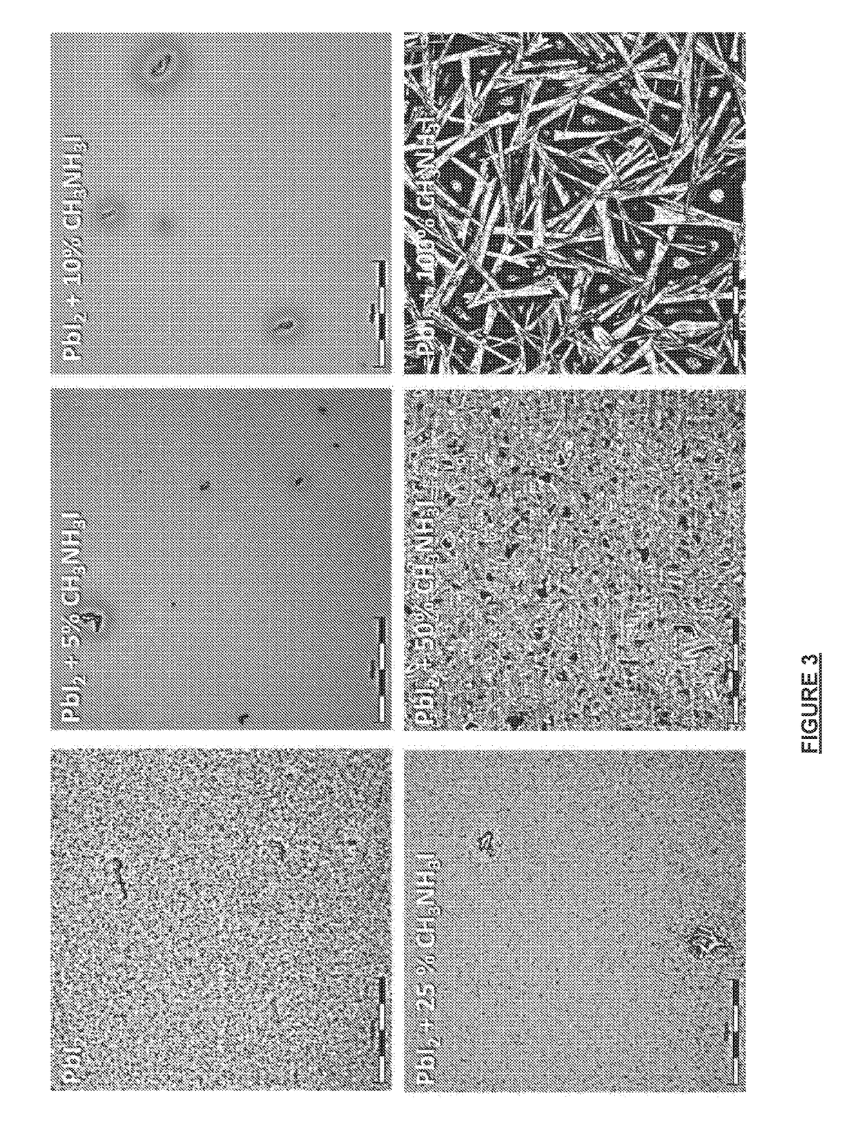
[0171]The perovskite photoactive layers were fabricated using a similar methodology as set out in Example 1. However, here the range of different PbI2 solution compositions were applied with and without an AX(CH3NH3I) additive, comprises (A) PbI2 solution (no CH3NH3I); (B) PbI2 with 30% CH3NH3I.

[0172]CH3NH3I solution (10 mg / mL) in 2-propanol was prepared for perovskite conversion. The PbI2 layers were dipped into the CH3NH3I solution for 3 min, rinsed with 2-propanol before the film dried, and then the solvent was quickly removed by N2 gas-blowing. The reaction speed of PbI2 films without and with 30 mol % CH3NH3I were tested by timing the formation of perovskite layer formation by monitoring absorbance change during conversion. A white LED was illuminated to a beaker with CH3NH3I solution and light transmission through the beaker was monitored by a photodiode. PbI2 films with and without an AX(CH3NH3I) additive were dipped to ...

example 3

Coated Perovskite Solar Cell Devices

Photoactive Layer Fabrication:

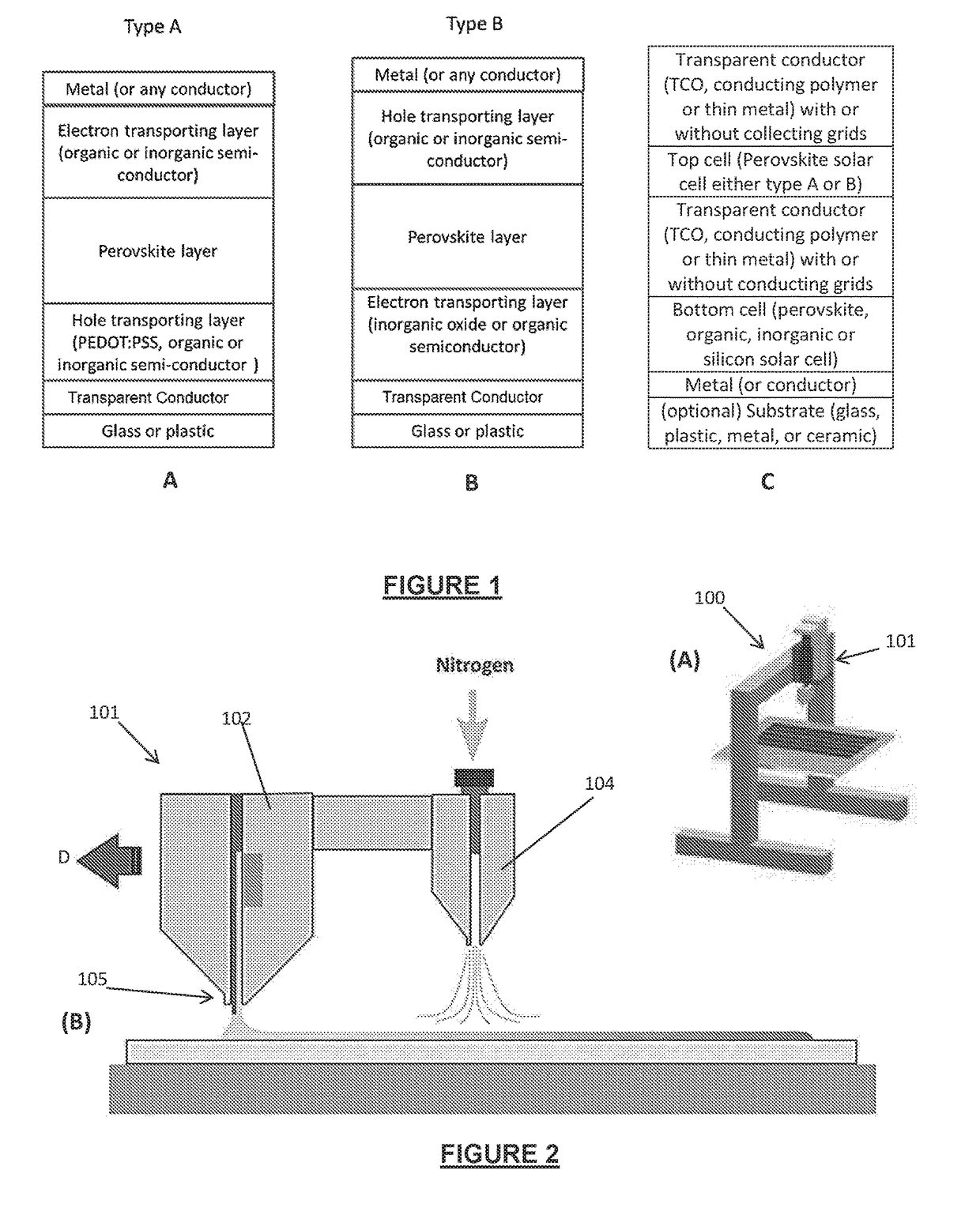
[0174]The perovskite photoactive layers were fabricated using a similar methodology as set out in Example 1. However, in this run the PbI2 layers were fabricated by slot die coating with gas quenching as described in relation to FIG. 2 above and taught in Hwang et al, Toward Large Scale Roll-to-Roll Production of Fully Printed Perovskite Solar Cells DOI: 10.1002 / adma.201404598 again, the contents of which are to be understood to be incorporated into this specification by this reference. Furthermore, in this experimental run, the PbI2 layer were formed using four different techniques:[0175]A). Slot die coated PbI2 layer without CH3NH3I, air dried for 10 minutes;[0176]B). Slot die coated PbI2 layer without CH3NH3I, stored in a small chamber for solvent vapour soaking for 10 minutes;[0177]C). Slot die coated PbI2 layer with CH3NH3I, air dried for 10 minutes; and[0178]D). Slot die coated PbI2 layer with CH3NH3I, stored in...

example 5

Coated Perovskite Solar Cells with Extra Additive

Photoactive Layer Fabrication:

[0186]The perovskite photoactive layers were fabricated using a similar methodology as set out in Example 1. However, here extra polymer additive was added to PbI2 with 40 mol % CH3NH3I to improve processability further as described above and also in the Applicants pending international patent application No. PCT / AU2015 / 000100, published as WO2015127494A1, the contents of which are incorporated into this specification by this reference.

[0187]5 mg of polyvinlyacetate was added to 1 ml of 0.7 M PbI2 with 40 mol % CH3NH3I as a crystallization retardant. For these experiments a 200 μm gap between a meniscus guide and the substrate was used to maximize the wet film thickness. Coating was carried out at speed of 5 mm / s with 1 μL / cm2 solution feed with gas quenching as described in relation to FIG. 2 above and as taught in Hwang et al (see Example 1). Films were kept in open environment, i.e. no soaking process ...


PUM


Abstract

A process of forming a photoactive layer of a planar perovskite photoactive device comprising: applying at least one layer of a first precursor solution to a substrate to form a first precursor coating on at least one surface of the substrate, the first precursor solution comprising MX.sub.2 and AX dissolved in a first coating solvent, wherein the molar ratio of MX.sub.2:AX=1:n with 0<n<1; and applying a second precursor solution to the first precursor coating to convert the first precursor coating to a perovskite layer AMX.sub.3, the second precursor solution comprising AX dissolved in a second coating solvent, the first precursor solution reacting with the second precursor solution to form a perovskite layer AMX.sub.3 on the substrate, wherein A comprises an ammonium group or other nitrogen containing organic cation, M is selected from Pb, Sn, Ge, Ca, Sr, Cd, Cu, Ni, Mn, Co, Zn, Fe, Mg, Ba, Si, Ti, Bi, or In, X is selected from at least one of F, Cl, Br or I.

Description

CROSS-REFERENCE[0001]The present application claims priority from Australian provisional patent application No. 2015900169 filed on 21 Jan. 2015, the disclosure of which should be understood to be incorporated into this specification.TECHNICAL FIELD[0002]The present invention generally relates to a process of forming a photoactive layer of a planar perovskite photoactive device. The invention is particularly applicable for perovskite type solar cells and it will be convenient to hereinafter disclose the invention in relation to that exemplary application.BACKGROUND TO THE INVENTION[0003]The following discussion of the background to the invention is intended to facilitate an understanding of the invention. However, it should be appreciated that the discussion is not an acknowledgement or admission that any of the material referred to was published, known or part of the common general knowledge as at the priority date of the application.[0004]Photovoltaic (PV) cells that convert sunli...

Claims


Application Information

Patent Timeline
Patent Type & Authority Applications(United States)
IPC IPC(8): H01G9/00H01L51/00H01G9/20H01L51/42
CPCH01G9/0029H01L51/0007H01G9/2018H01G9/2072H01L51/0077H01G9/2095H01L51/4273H01L27/302H01L51/0004H01L51/005H01L51/4233H01L51/4246Y02E10/542Y02E10/549
Inventor VAK, DOOJINHEO, YOUN-JUNG
Owner COMMONWEALTH SCI & IND RES ORG
Why Eureka
Try Eureka