Ceramic capacitor

a ceramic capacitor and capacitor technology, applied in the field of ceramic capacitors, can solve the problems of not being suitable for being embedded in a substrate, multi-terminal capacitors, and difficult to suitably embed multi-terminal capacitors, and achieve the effect of low esl

Active Publication Date: 2017-11-30
MURATA MFG CO LTD
View PDF5 Cites 22 Cited by
  • Summary
  • Abstract
  • Description
  • Claims
  • Application Information

AI Technical Summary

Benefits of technology

[0022]According to various preferred embodiments of the present invention, it is possible to provide ceramic capacitors which are low in ESL and suitable for being built into a substrate.

Problems solved by technology

However, the multi-terminal capacitors described in Japanese Patent Application Laid-Open No. 2001-155962 and Japanese Patent Application Laid-Open No. 2001-102243 do not consider embedding in a substrate and electrical connection to wirings formed on the substrate.
Therefore, it is difficult to suitably embed the multi-terminal capacitors described in Japanese Patent Application Laid-Open No. 2001-155962 and Japanese Patent Application Laid-Open No. 2001-102243 in a substrate.
In other words, multi-terminal capacitors described in Japanese Patent Application Laid-Open No. 2001-155962 and Japanese Patent Application Laid-Open No. 2001-102243 are not suitable for being embedded in a substrate.
Accordingly, when the ground terminal is formed from one side surface to the other side surface so as to extend over the principal surface, flatness of the external electrode may be impaired.
When such a multilayer ceramic capacitor is embedded in the built-in electronic component substrate, there is a possibility that the electrical connection between the external electrodes and the via hole electrodes is deteriorated.
Accordingly, there is a possibility that defective connection between the multilayer ceramic capacitor and the built-in electronic component substrate occurs.

Method used


Image

  • Ceramic capacitor
  • Ceramic capacitor
  • Ceramic capacitor

Examples


second preferred embodiment

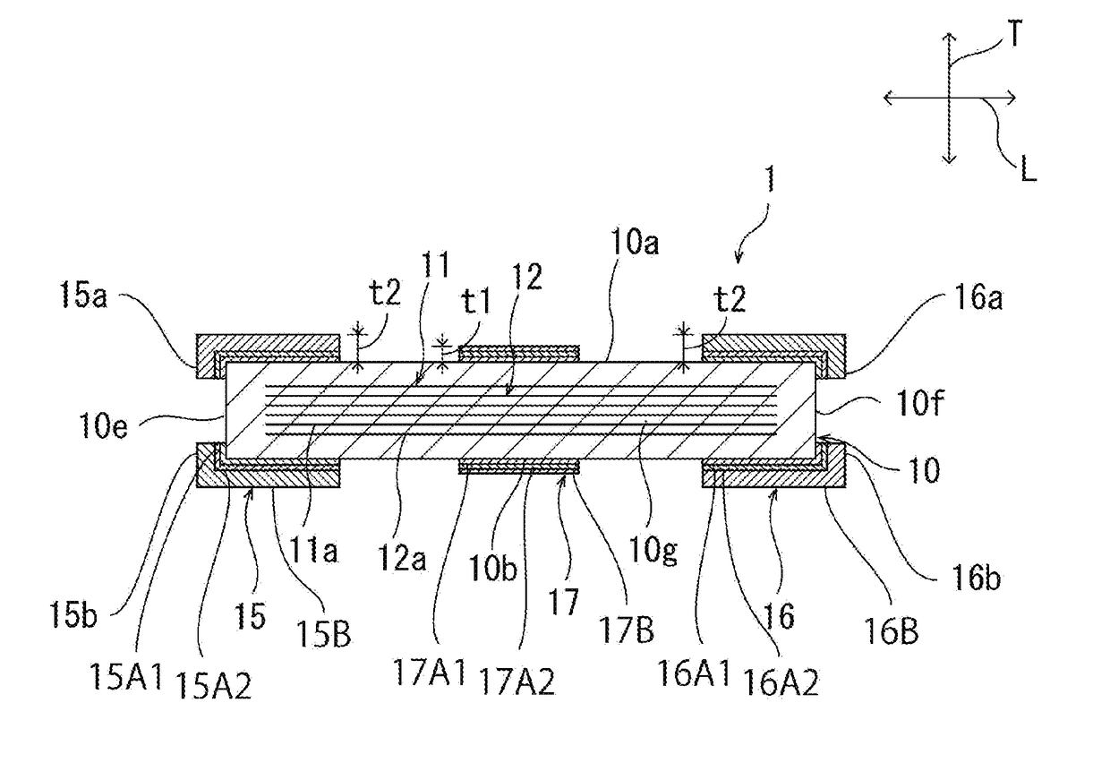
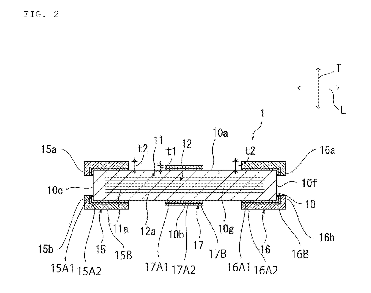
[0106]FIG. 10 and FIG. 11 are each a schematic cross-sectional view of a capacitor according to a second preferred embodiment of the present invention. In the first preferred embodiment, an example has been described in which the first external electrode 15 includes the first portion 15a, the second portion 15b, the third portion 15c and the fourth portion 15d, and the second external electrode 16 includes the fifth portion 16a, the sixth portion 16b, the seventh portion 16c and the eighth portion 16d. However, the present invention is not limited to this configuration.

[0107]As with the ceramic capacitor 1a shown in FIG. 10 and FIG. 11, the first to third external electrodes 15 to 17 do not have to have the first portion to the eighth portion 15a to 15d, 16a to 16d. Specifically, in the ceramic capacitor 1a, the first external electrode 15 is not disposed on a ridge which the first principal surface 10a defines with the first end surface 10e, on a ridge which the second principal su...

example 1

[0109]1000 pieces of capacitors having the substantially same constitution as in the ceramic capacitor 1 of the first preferred embodiment were prepared under the following conditions using the manufacturing method described in the first preferred embodiment.

Conditions:

[0110]Dimension of a ceramic capacitor (standard dimension): L×W×T=1.000 mm×0.600 mm×0.220 mm

[0111]Thickness of a capacitor main body: 200 μm

[0112]Ceramic material: BaTi2O3

[0113]Capacitance: 1 μF

[0114]Rated voltage: 6.3V

[0115]Sputtering electrode film: NiCr film, NiCu film (two layer structure)

[0116]Thickness of a NiCr film: 150 nm

[0117]Thickness of a NiCu film: 150 nm

[0118]Plated layer: one Cu plated layer

[0119]Thickness of a plated layer: 10 μm

experimental example

[0127]A plurality of capacitors in which their constitutions were substantially the same as that of the ceramic capacitor 1 of the first preferred embodiment and the thicknesses of the sputtering electrode films are thicknesses shown in Table 2, were prepared as samples using the manufacturing method described in the first preferred embodiment, and flatness of the external electrode, adhesion between the sputtering electrode film and the capacitor main body, and chip of the external electrode were evaluated. In addition, sputtering conditions were as follows.

Sputtering Conditions

[0128]Sputtering electrode film: laminated body of a NiCr film and a NiCu film

[0129]Apparatus: batch type sputtering apparatus

[0130]Ar gas flow rate: 0.8 cc / min

[0131]Pressure in film forming chamber: 0.33 Pa

Measurement Method of Thickness of Sputtering Electrode Film

[0132]A side surface of each of the ceramic capacitors prepared in Experiment Examples was polished until a width dimension of the ceramic capac...


PUM


Abstract

A ceramic capacitor which is low in ESL and suitable for being built into a substrate includes a first external electrode, a second external electrode and a third external electrode. Each of the first, second and third external electrodes include a sputtering electrode film. Each of the outermost layers of the first, second and third external electrodes contains Cu.

Description

CROSS REFERENCE TO RELATED APPLICATIONS[0001]This application claims the benefit of priority to Japanese Patent Application No. 2016-108584 filed on May 31, 2016. The entire contents of this application are hereby incorporated herein by reference.BACKGROUND OF THE INVENTION1. Field of the Invention[0002]The present invention relates to a ceramic capacitor.2. Description of the Related Art[0003]In recent years, the demand for miniaturization and thinning of information terminal devices such as mobile phones and mobile music players is increasing. Associated with this, downsizing is also increasingly required in substrates to be installed in electronic devices and electronic components to be installed in substrates. High density mounting of electronic components to be mounted on a substrate is also increasingly required. In order to further downsize electronic components, a built-in electronic component substrate in which an electronic component is embedded has been developed (e.g., J...

Claims


Application Information

Patent Timeline
Patent Type & Authority Applications(United States)
IPC IPC(8): H01G4/12H01G4/005H01G4/30C23C14/34
CPCH01G4/1209H01G4/302C23C14/34H01G4/005H01G4/306C23C14/185H01G4/232
Inventor TANAKA, YUICHIRO
Owner MURATA MFG CO LTD
Why Eureka
Try Eureka