High-contrast photonic crystal "or," "not" and "xor" logic gate

a photonic crystal, logic gate technology, applied in logic circuits, pulse techniques, instruments, etc., can solve the problems of difficult manufacturing of quantum optical logic devices and nanomaterial optical logic devices, and achieve high contrast of high and low logic output, easy integration with other optical logic elements, and compact structure

Inactive Publication Date: 2017-12-07
OUYANG ZHENGBIAO
View PDF11 Cites 1 Cited by
  • Summary
  • Abstract
  • Description
  • Claims
  • Application Information

AI Technical Summary

Benefits of technology

[0007]The present invention is aimed at overcoming the defects of the prior art and providing a high-contrast PhC “OR”, “NOT” and “XOR” logic

Problems solved by technology

For modern manufacturing processes, however, the quantum optical logic devices and the nano material optical logic devices are very

Method used


Image

  • High-contrast photonic crystal "or," "not" and "xor" logic gate
  • High-contrast photonic crystal "or," "not" and "xor" logic gate
  • High-contrast photonic crystal "or," "not" and "xor" logic gate

Examples


embodiment 1

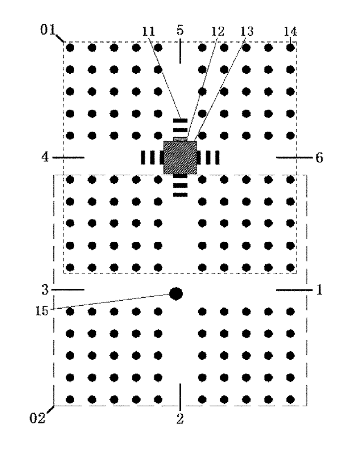
[0058]Referring to that shown in FIG. 1, the lattice constant d is 1 μm; the operating wavelength is 2.976 μm; the radius of the circular high-refractive-index linear-dielectric pillar 14 is 0.18 μm; the long sides of the first rectangular high-refractive-index linear-dielectric pillar 11 are 0.613 μm, and the short sides are 0.1621 μm; the size of the second rectangular high-refractive-index linear-dielectric pillar 12 is the same as that of the first rectangular high-refractive-index linear-dielectric pillar 11; the side length of the square nonlinear-dielectric pillar 13 is 1.5 μm, and the third-order nonlinear coefficient is 1.33×10⁻² μm2 / V2; and the distance between every two adjacent rectangular linear-dielectric pillars is 0.26681 μm; the radius of the circular linear-dielectric pillar 15 is 0.292 μm; Referring to the structure shown in FIG. 1, reference-light E1 and E2 are respectively input to the port 1 and the port 4, wherein E1=E2=1; an Input Signal shown in FIG. 5 is in...

embodiment 2

[0061]Referring to that shown in FIG. 1, the lattice constant d is 1 μm; the operating wavelength is 2.976 μm; the radius of the circular high-refractive-index linear-dielectric pillar 14 is 0.18 μm; the long sides of the first rectangular high-refractive-index linear-dielectric pillar 11 are 0.613 μm, and the short sides are 0.162 μm; the size of the second rectangular high-refractive-index linear-dielectric pillar 12 is the same as that of the first rectangular high-refractive-index linear-dielectric pillar 11; the side length of square nonlinear-dielectric pillar 13 is 1.5 μm, and the third-order nonlinear coefficient is 1.33×10⁻² μm2 / V2; and the distance between every two adjacent rectangular linear-dielectric pillars is 0.2668 μm; the radius of the circular nonlinear-dielectric pillar 15 is 0.292 μm. Referring to the structure shown in FIG. 1, reference-light E is input to the port 4, wherein E=1; port 1 and port 2 signals shown in FIG. 6 are respectively input to the port 1 an...

embodiment 3

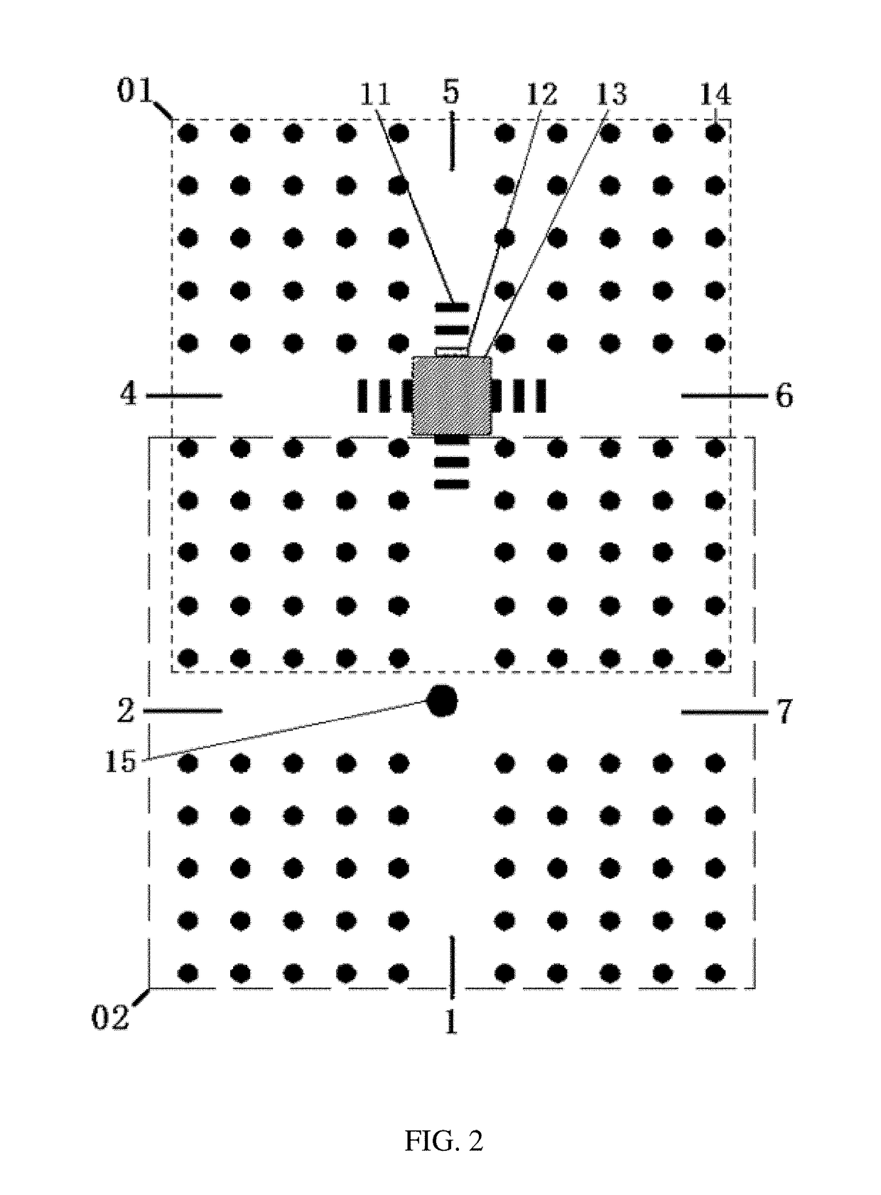
[0066]Referring to that shown in FIG. 2, the lattice constant d is 1 μm; the operating wavelength is 2.976 μm; the radius of the circular high-refractive-index linear-dielectric pillar 14 is 0.18 μm; the long sides of the first rectangular high-refractive-index linear-dielectric pillar 11 are 0.613 μm, and the short sides are 0.162 μm; the size of the second rectangular high-refractive-index linear-dielectric pillar 12 is the same as that of the first rectangular high-refractive-index linear-dielectric pillar 11; the side length of square nonlinear-dielectric pillar 13 is 1.5 μm, and the third-order nonlinear coefficient is 1.33×10⁻² μm2 / V2; and the distance between every two adjacent rectangular linear-dielectric pillars is 0.2668 μm; the radius of the circular linear-dielectric pillar 15 is 0.292 μm.

[0067]Referring to the structure shown in FIG. 1, reference-light E is input to the port 4, wherein E=1; port 1 and port 2 signals shown in FIG. 7 are respectively input to the port 1 ...


PUM


Abstract

The present invention discloses an high-contrast photonic crystal “OR”, “NOT” and “XOR” logic gate, comprising a six-port two-dimensional photonic crystal, a nonlinear cavity unit and a cross-waveguide logic gate unit; the high-contrast photonic crystal “OR” logic gate includes a first reference-light input port, two first idle ports, two first signal-input ports and a first signal-output port; the high-contrast photonic crystal “NOT” logic gate includes two second reference-light input ports, two second idle ports, a second signal-input port and a second signal-output port; and the high-contrast photonic crystal “XOR” logic gate includes a three reference-light input port, two three-idle ports, two three-signal input ports and a three-signal output port; the cross-waveguide logic gate unit is arranged with different input or output ports; and the nonlinear cavity unit is coupled with the cross-waveguide logic gate unit. The structure of the present invention is easy to integrate with other optical logic elements.

Description

CROSS-REFERENCE TO RELATED APPLICATION[0001]This application is a continuation application of PCT Application No. PCT / CN2015 / 097846 filed on Dec. 18, 2015 which claims priority to Chinese Application No. 201410797514.4 filed on Dec. 19, 2014, the entire contents of which are hereby incorporated by reference.FIELD OF THE INVENTION[0002]The present invention relates generally to two-dimensional (2D) photonic crystals (PhCs), nonlinear optics and optical “OR,”“NOT” AND “XOR” logic gates.BACKGROUND OF THE INVENTION[0003]In 1987, the concept of PhC was proposed separately by E. Yablonovitch from United States Bell Labs who discussed how to suppress spontaneous radiation and by S. John from Princeton University who made discussions about photonic localization. A PhC is a material structure in which dielectric materials are arranged periodically in space, and is usually an artificial crystal comprising of two or more materials having different dielectric constants.[0004]With the emergence ...

Claims


Application Information

Patent Timeline
IPC IPC(8): G02F3/00G02B6/122G02B6/125G02F1/365
CPCG02F3/00G02F1/365G02B6/1223G02F2201/06G02B6/125G02F2202/32G02B6/1225G02F1/35G02F1/3501G02F1/3511
Inventor OUYANG, ZHENGBIAOYU, QUANQIANG
Owner OUYANG ZHENGBIAO
Why Eureka
Try Eureka