Check patentability & draft patents in minutes with Patsnap Eureka AI!

Single-electron transistor with self-aligned coulomb blockade

a single-electron transistor and coulomb blockade technology, applied in the field of single-electron transistors, can solve the problems of difficult to reliably manufacture the coulomb blockade in the set, the device approaches the limit of what can be achieved, and the conventional set needs very low temperatures to operate correctly

Active Publication Date: 2017-12-07
IBM CORP
View PDF4 Cites 3 Cited by
  • Summary
  • Abstract
  • Description
  • Claims
  • Application Information

AI Technical Summary

Benefits of technology

The patent describes a method of making a transistor by creating a structure on a thin layer of materials. This structure includes a gate, source and drain regions, and a channel region, all separated by notches. The method also involves adding more material on top of the thin layer to form the source and drain regions. A semiconductor device that includes this structure on a buried insulator is also described. The invention allows for the creation of transistors with improved performance and efficiency.

Problems solved by technology

As conventional fabrication methods improve, and logic devices such as transistors become smaller, devices approach a limit of what can be achieved using standard complementary metal-oxide semiconductor (CMOS) processes.
However, conventional SETs need very low temperatures to operate correctly.
In addition, it is difficult to manufacture the Coulomb blockade in an SET reliably.

Method used


Image

  • Single-electron transistor with self-aligned coulomb blockade
  • Single-electron transistor with self-aligned coulomb blockade
  • Single-electron transistor with self-aligned coulomb blockade

Examples


Embodiment Construction

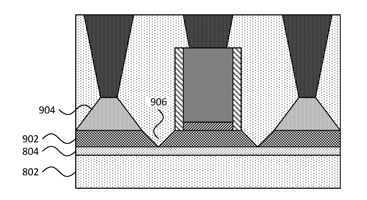
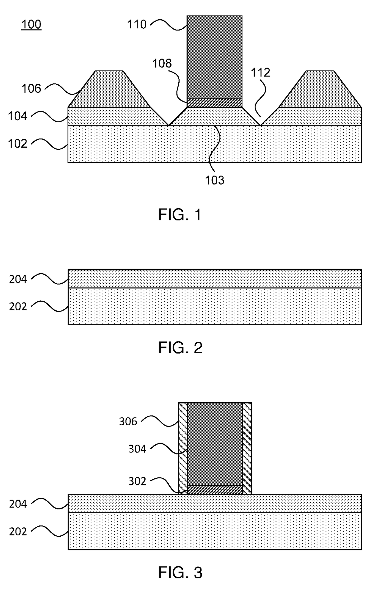
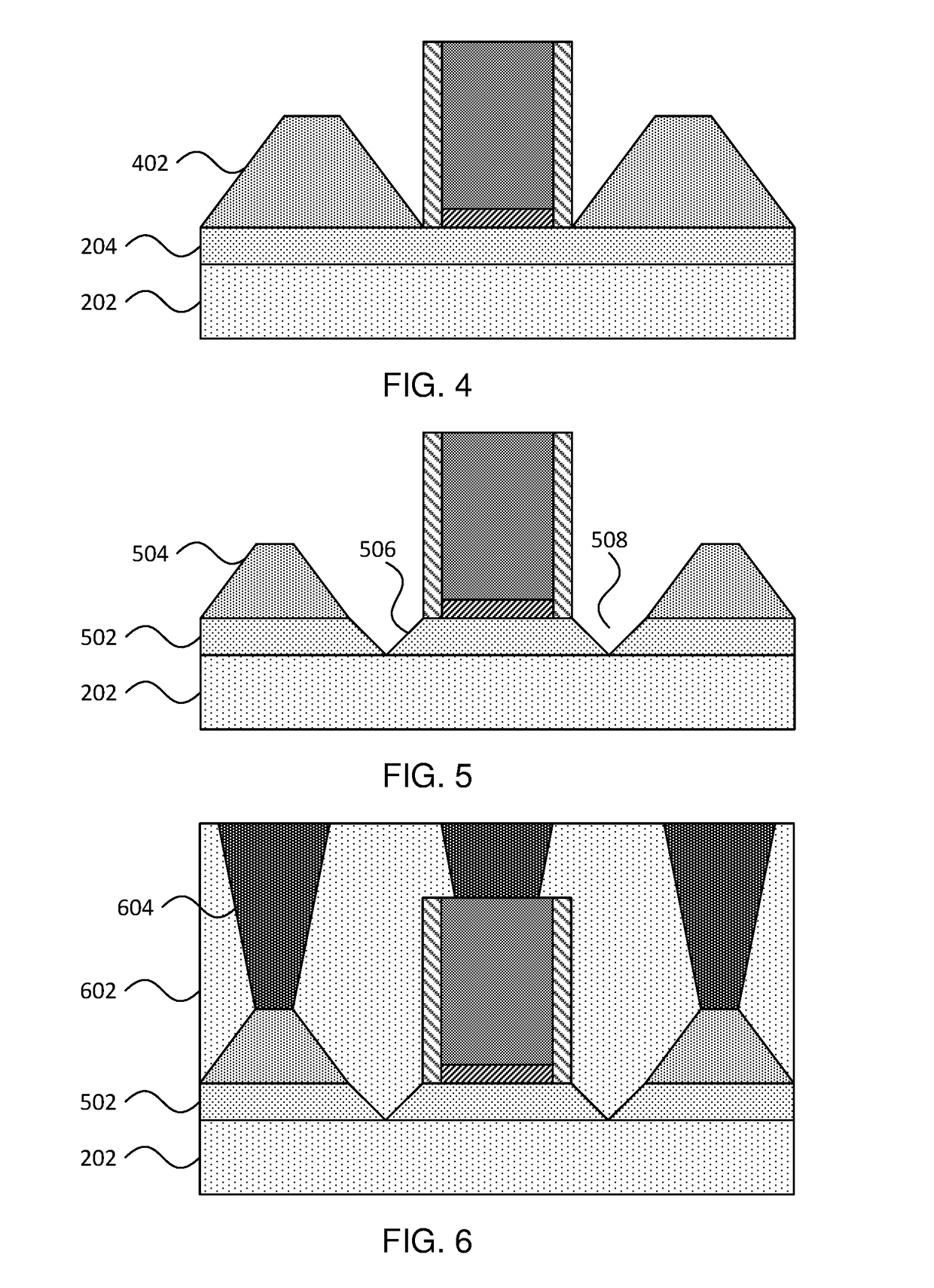
[0017]Embodiments of the present invention provide single-electron transistors (SETs) that operate at high temperature and uses complementary metal oxide semiconductor (CMOS) fabrication processes to control the dimensions of the Coulomb blockade. A channel is formed with a length and width being controlled by sidewall image transfer and the Coulomb blockade thickness being controlled by extremely thin semiconductor-on-insulator deposition. The Coulomb blockade is formed as notches between the channel and the source and drain regions.

[0018]Referring now to FIG. 1, a diagram of an SET 100 is shown. Starting from an extremely thin semiconductor-on-insulator substrate, a channel 103 and source / drain regions 104 are formed on a buried dielectric layer 102. Epitaxially grown source / drain extensions 106 are formed on the top surfaces of the source / drain regions 104. A gate conductor 110 and gate dielectric 108 are formed on the channel 103. Notches 112 are cut to separate the channel 103 ...


PUM


Abstract

Semiconductor devices and methods of making the same include forming a gate structure on a thin semiconductor layer. Additional semiconductor material is formed on the thin semiconductor layer. The thin semiconductor layer is etched back and the additional semiconductor material to form source and drain regions and a channel region, with notches separating the source and drain region from the channel region.

Description

BACKGROUNDTechnical Field[0001]The present invention relates to semiconductor devices and, more particularly, to single-electron transistors.Description of the Related Art[0002]As conventional fabrication methods improve, and logic devices such as transistors become smaller, devices approach a limit of what can be achieved using standard complementary metal-oxide semiconductor (CMOS) processes. Single-electron transistors (SETs), which operate by quantum tunneling effects, can provide logic devices at even smaller scales than CMOS. However, conventional SETs need very low temperatures to operate correctly. In addition, it is difficult to manufacture the Coulomb blockade in an SET reliably.SUMMARY[0003]A method for forming a transistor includes forming a gate structure on a thin semiconductor layer. Additional semiconductor material is formed on the thin semiconductor layer. The thin semiconductor layer is etched back and the additional semiconductor material to form source and drain...

Claims


Application Information

Patent Timeline
IPC IPC(8): H01L29/76H01L29/423H01L29/165H01L29/10H01L29/08H01L29/06H01L21/306H01L29/66H01L21/02
CPCH01L29/7613H01L21/30604H01L29/42372H01L29/0649H01L29/1033H01L29/165H01L29/66439H01L29/0847H01L21/02532B82Y10/00H01L29/1037H01L29/127H01L29/4232
Inventor CAO, QINGCHENG, KANGGUOLI, ZHENGWENLIU, FEI
Owner IBM CORP
Features
  • R&D
  • Intellectual Property
  • Life Sciences
  • Materials
  • Tech Scout
  • Unparalleled Data Quality
  • Higher Quality Content
  • 60% Fewer Hallucinations
Learn More