Semiconductor Device For Measuring Ultra Small Electrical Currents And Small Voltages

a technology of electrical current and small voltage, applied in the direction of ac/dc measuring bridge, reference comparison, instruments, etc., can solve the problems of unpractical methods and single electrical charge carriers, and achieve the effects of high kinetic energy, easy measurement, and high gain

Inactive Publication Date: 2010-01-21
ECOLE POLYTECHNIQUE FEDERALE DE LAUSANNE (EPFL)
View PDF10 Cites 35 Cited by
  • Summary
  • Abstract
  • Description
  • Claims
  • Application Information

AI Technical Summary

Benefits of technology

[0017]The term “avalanche diode” is widely known and means a diode formed as a PN junction between p-type semiconductor material and n-type semiconductor material and operated biased with a reverse voltage for making use of the avalanche effect. The avalanche effect occurs when a single free charge carrier reaching the high electrical field region of the PN junction acquires a sufficiently high kinetic energy to create an electron-hole pair by impact ionization. The free carriers created thereby also accelerate in the strong electrical field and cause the creation of more electron-hole pairs which undergo the same multiplication process. The result of the avalanche effect is that a free carrier reaching the depletion region of the avalanche diode produces a lot of electrons and holes which result in a strong current pulse that can easily be measured. In order to achieve high gain, the avalanche diode is operated with a high reverse-bias voltage. However, the gain may be further increased if the avalanche diode is operated in the Geiger mode. In this mode the avalanche diode is reverse-biased above the breakdown voltage. Any triggered avalanche effect leads to an increasing avalanche current that is maintained as long as the bias voltage stays above the breakdown voltage. The quenching and recharging circuit serves to stop the avalanche effect after a certain time delay so that the semiconductor device is ready to detect a next free carrier. The quenching and recharging circuit may be a passive circuit including, for example, a resistor. The avalanche current discharges the diode capacitance because it is much larger than the current allowed to flow through the quenching resistor, and thus lowers the bias voltage of the PN junction until the avalanche effect stops. As soon as the avalanche current stops, the reverse-bias across the PN junction increases again until it reaches the level of the supply voltage. The quenching and recharging circuit may also be an active circuit that achieves the same functions with active components.
[0018]The result of this process is a short current pulse crossing the base-collector junction. It may be detected as a voltage drop at the node between the collector of the bipolar transistor and the quenching and recharging circuit. The detection of this voltage drop is straightforward and therefore the output terminal is preferably connected to this node. Every triggered avalanche effect produces a voltage drop at this node and looks like a voltage pulse that may be further processed. It may be fed for example to a counter. However, the avalanche current could also be detected in another way, e.g., as an increase in the current flowing through the quenching and recharging circuit.

Problems solved by technology

With this measurement technique, single electrical charge carriers cannot be detected because their signals disappear in the noise.
However, the need for cryogenic temperatures makes this method unpractical.

Method used


Image

  • Semiconductor Device For Measuring Ultra Small Electrical Currents And Small Voltages
  • Semiconductor Device For Measuring Ultra Small Electrical Currents And Small Voltages
  • Semiconductor Device For Measuring Ultra Small Electrical Currents And Small Voltages

Examples


Embodiment Construction

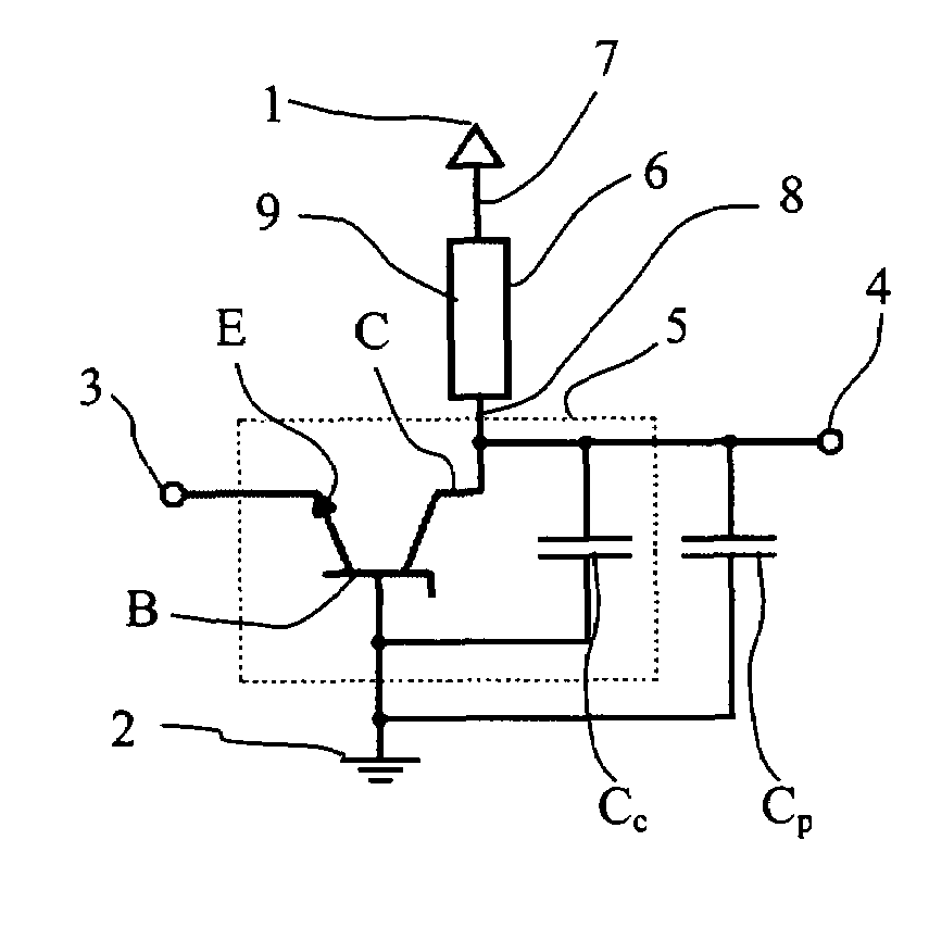
[0038]FIG. 1 shows a circuit diagram of the semiconductor device according to a first embodiment of the invention. The semiconductor device has a first voltage supply terminal 1, a second voltage supply terminal 2, an input terminal 3 and an output terminal 4. The semiconductor device comprises a bipolar transistor 5 having a base B, an emitter E and a collector C, and a quenching and recharging circuit 6. The emitter E is directly connected to the input terminal 3, the collector C is directly connected to the output terminal 4 and the base B is connected to the second voltage supply terminal 2. The quenching and recharging circuit 6 is a passive circuit having a first terminal 7 connected to the first supply voltage terminal 1 and a second terminal 8 connected to the collector C. In the present embodiment the quenching and recharging circuit 6 is an ohmic resistor 9. The capacitances Cc and Cp are not real capacitors but inherently present capacitances. Their influence on the prope...


PUM


Abstract

A semiconductor device for measuring ultra low currents down to the level of single electrons or low voltages comprises a first and a second voltage supply terminal, an input terminal for receiving an electrical current or being supplied with a voltage to be measured, a bipolar transistor having a base, an emitter and a collector, wherein a first PN junction is formed between the base and the collector and a second PN junction is formed between the base and the emitter, wherein the emitter is coupled to the input terminal and the base is coupled to the second voltage supply terminal, and wherein the first PN junction is designed for reverse biased operation as an avalanche diode, and a quenching and recharging circuit having a first terminal coupled to the first voltage supply terminal and a second terminal coupled to the collector of the bipolar transistors, the quenching and recharging circuit permitting operation of the first PN junction reverse biased above the breakdown voltage of the first PN junction.

Description

CROSS REFERENCE TO RELATED APPLICATIONS[0001]The present application is related to and claims priority based upon PCT Patent Application No. PCT / EP2007 / 064100 entitled “Semiconductor Device For Measuring Ultra Small Electrical Currents And Small Voltages”, filed Dec. 17, 2007, which, in turn, claims priority from European Patent Application No. 06126681.3, filed on Dec. 20, 2006, the disclosure of both of which is hereby incorporated herein by reference.TECHNICAL FIELD[0002]The present invention is directed to a semiconductor device for measuring ultra-small electrical currents down to the level of measuring even single electrical charge carriers and for measuring small voltages.BACKGROUND OF THE INVENTION[0003]Conventional current measurements involve measuring the voltage drop across a resistor. With this measurement technique, single electrical charge carriers cannot be detected because their signals disappear in the noise.[0004]Low current measurement by electron counting has al...

Claims


Application Information

Patent Timeline
Patent Type & Authority Applications(United States)
IPC IPC(8): G01R19/00
CPCG01R19/0092H01L29/0804H01L29/7322H01L29/7313H01L29/0821
Inventor LANY, MARCPOPOVIC, RADIVOJE
Owner ECOLE POLYTECHNIQUE FEDERALE DE LAUSANNE (EPFL)
Why Eureka
Try Eureka