
Low capacitance optoelectronic device

a low capacitance, optoelectronic device technology, applied in the direction of lasers, semiconductor laser structural details, semiconductor lasers, etc., can solve the problems of parasitic capacitance, introduction of additional capacitance, and limiting the high-speed performance of vcsels and photodiodes, etc., to achieve the effect of low capacitan

Active Publication Date: 2017-12-28
VI SYST GMBH +1
View PDF0 Cites 19 Cited by
  • Summary
  • Abstract
  • Description
  • Claims
  • Application Information

AI Technical Summary

Benefits of technology

This patent describes a method of creating an optoelectronic semiconductor device by isolating a section of it from the rest of the device using a continuous layer of oxide or a round trench. This results in low capacitance pads and a low total capacitance for the device. The technical effect is improved performance and efficiency of the optoelectronic device.

Problems solved by technology

The major factor limiting the high-speed performance of the VCSELs as well as photodiodes is the parasitic capacitance.
Third, the devices with a low capacitance require epitaxial growth on a semi-insulating substrate and making a contact to the bottom distributed Bragg reflector (DBR) from the top through a trench etched down to a doped buffer layer grown on a semi-insulating substrate, wherein both contact pads are formed on the same level on top of the device.
However, contact pads introduce additional capacitance.
This approach requires rather complex processing whereas such dielectric is often fragile, also showing a poor adhesion to the semiconductor material resulting in lift-off of the contact pads once bonding is attempted.
Such an approach does not enable fabricating low capacitance VCSELs.
Such a design has several critical issues in the production.
There are adhesion problems of the organic dielectric layer on the semiconductor as well as of other layers like metal on top of the organic dielectric layer which may result in delamination in bonding technology as well as weakness in long term stability.

Method used


Image

  • Low capacitance optoelectronic device
  • Low capacitance optoelectronic device
  • Low capacitance optoelectronic device

Examples


Embodiment Construction

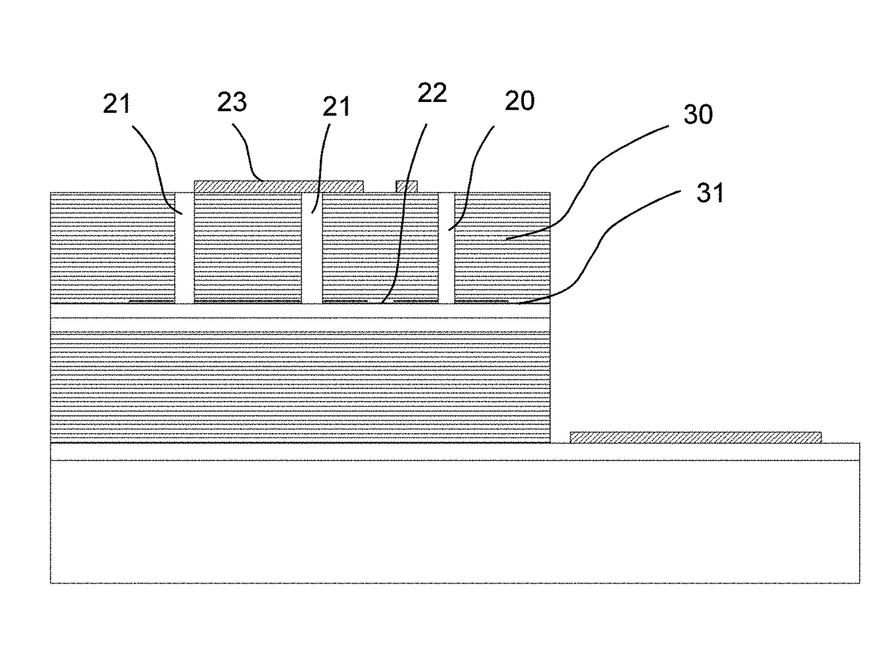
[0021]FIGS. 3a and 3b illustrate schematically one embodiment of the present invention. Holes (20) or trenches (21) are etched through the top DBR (30) of a VCSEL. It is even possible to etch further through the p-n junction of a VCSEL. The etching is performed through one or several layers of AlGaAs (31) with a high Aluminum content which are subject to selective oxidation. The oxidation process starts from the etched holes and results in the formation of the oxide layer or oxide layers with a certain extension around the holes or trenches (20a, 21a). The positions of the holes, the shape of the holes and the distance between the holes as well as the extension of oxidation are preferably selected such that the oxide areas generated by neighboring holes overlap (20b) and leaving only some small non-oxidized areas in between (22). These non-oxidized areas will form the apertures for the current flow and for the propagation of light. One may define the oxidized section of the device b...


PUM


Abstract

An optoelectronic semiconductor device is disclosed wherein the device is a vertical-cavity surface-emitting laser or a photodiode containing a section, the top part of which is electrically isolated from the rest of the device. The electric isolation can be realized by etching a set of holes and selective oxidation of AlGaAs layer or layers such that the oxide forms a continuous layer or layers everywhere beneath the top surface of this section. Alternatively, a device can be grown epitaxially on a semi-insulating substrate, and a round trench around a section of the device can be etched down to the semi-insulating substrate thus isolating this section electrically from the rest of the device. Then if top contact pads are deposited on top of the electrically isolated section, the pads have a low capacitance, and a pad capacitance below two hundred femto-Farads, and the total capacitance of the device below three hundred femto-Farads can be reached.

Description

REFERENCE TO RELATED APPLICATIONS[0001]This application claims an invention, which was disclosed in Provisional Application No. 62 / 186,279, filed Jun. 29, 2015, entitled “Low Capacitance Vertical-Cavity Surface-Emitting Laser”. The benefit under 35 USC §119(e) of the United States provisional application is hereby claimed, and the aforementioned application is hereby incorporated herein by reference.BACKGROUND OF THE INVENTIONField of the Invention[0002]The invention pertains to the field of optoelectronic devices. More particularly, the invention pertains to vertical-cavity surface-emitting lasers and photodiode s.Description of Related Art[0003]Very fast optoelectronic devices are key components of the high-speed optical communication in High Power Computers, data centers, routers and all kinds of networks. It is necessary to apply for optical fiber connections very fast edge emitting lasers as well as Vertical Cavity Surface Emitting Lasers (VCSEL) as transmitters and very fast p...

Claims


Application Information

Patent Timeline
Patent Type & Authority Applications(United States)
IPC IPC(8): H01S5/22H01S5/187H01S5/183H01S5/042H01S5/30H01S5/02
CPCH01S5/2214H01S5/3054H01S5/305H01S5/0208H01S5/183H01S5/2202H01S5/18327H01S5/0421H01S5/18313H01S5/32H01S5/18308H01S5/18316H01S5/187H01L31/00H01S5/06226H01S5/1833H01L31/022408H01L31/0352H01L31/105H01L31/18H01S5/04257H01S2301/176H01S5/0262H01S5/04256
Inventor KROPP, JOERG-REINHARDTLEDENTSOV, NIKOLAYSHCHUKIN, VITALY
Owner VI SYST GMBH
Learn More