

Method for creating patterns
a pattern and pattern technology, applied in the field of structures, can solve the problems of reducing the dimensions of the pattern, the difficulty of being able to actually align the pattern with enough accuracy during successive photolithography operations, and the qualitative nature of the technique, so as to achieve good size control, simple and reliable solution, and good surface state
- Summary
- Abstract
- Description
- Claims
- Application Information
AI Technical Summary
Benefits of technology
Problems solved by technology
Method used
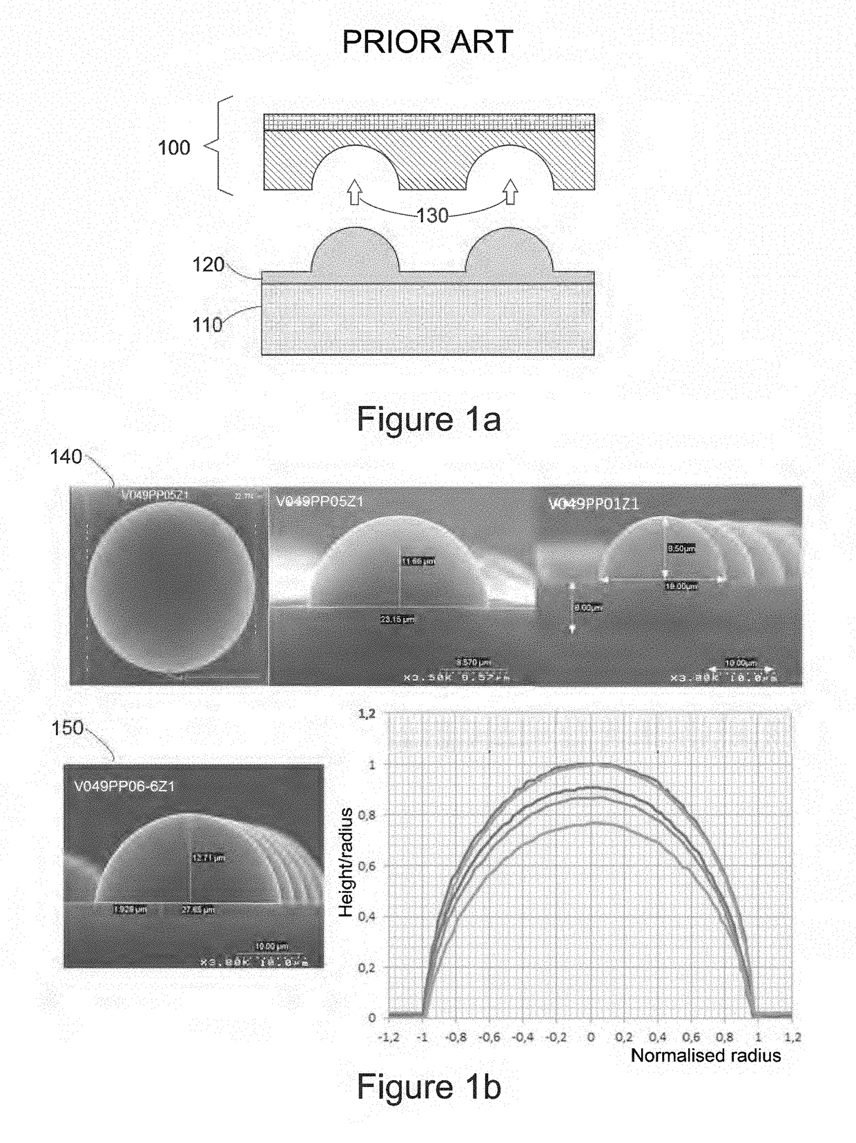
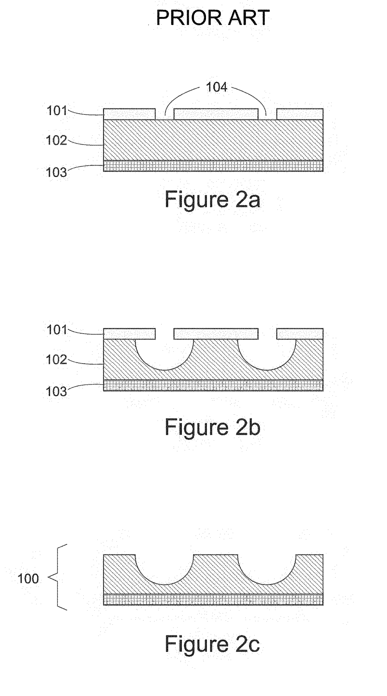
Image

Examples
Embodiment Construction
[0050]Before starting a detailed review of embodiments of the invention, optional features that can optionally be used in combination or alternatively are listed below:
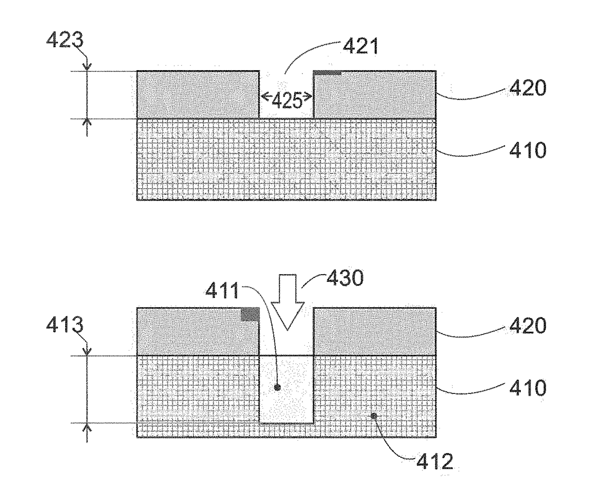
[0051]According to one embodiment, the step of enlarging the at least one pattern comprises anisotropic etching the masking layer, the main direction of which is parallel to a plane in which the layer to be etched mainly extends. This etching etches the masking layer selectively with respect to the layer to be etched.
[0052]The step of enlarging the at least one pattern of the masking layer does not etch the layer to be etched.
[0053]According to one embodiment, the stack comprises a buffer layer positioned between the masking layer and the layer to be etched.
[0054]According to one embodiment, the buffer layer covers the layer to be etched during the implantation.
[0055]Thus, the buffer layer remains above the layer to be etched during the step of modification via implantation, Thus, the elements of the masking layer tha...
PUM
| Property | Measurement | Unit |
|---|---|---|
| thickness | aaaaa | aaaaa |
| thickness | aaaaa | aaaaa |
| diameter | aaaaa | aaaaa |
Abstract
Description
Claims
Application Information