Fin field effect transistor (FET) (finfet) complementary metal oxide semiconductor (CMOS) circuits employing single and double diffusion breaks for increased performance

a field effect transistor and complementary metal oxide semiconductor technology, applied in the field of fets, can solve the problems of increased current leakage, degrade performance, and complex functionality of electronic devices, and achieve the effects of improving performance, increasing performance, and increasing performan

Active Publication Date: 2018-01-04
QUALCOMM INC
View PDF1 Cites 39 Cited by
  • Summary
  • Abstract
  • Description
  • Claims
  • Application Information

AI Technical Summary

Benefits of technology

[0008]Aspects disclosed herein include Fin Field Effect Transistor (FET) (FinFET) complementary metal oxide semiconductor (CMOS) circuits employing single and double diffusion breaks for increased performance In one aspect, a FinFET CMOS circuit employing single and double diffusion breaks is provided. The FinFET CMOS circuit includes a P-type FinFET that includes a first Fin formed from a semiconductor substrate and corresponding to a P-type semiconductor material (P-type) diffusion region. The FinFET CMOS circuit also includes an N-type FinFET that includes a second Fin formed from the semiconductor substrate and corresponding to an N-type semiconductor material (N-type) diffusion region. To electrically isolate the P-type FinFET, first and second single diffusion break (SDB) isolation structures are formed in the first Fin on either side of a gate of the P-type FinFET. To electrically isolate the N-type FinFET, first and second double diffusion break (DDB) isolation structures are formed in the second Fin on either side of a gate of the N-type FinFET. Employing SDB and DDB isolation structures allows the P-type FinFET and the N-type FinFET to each achieve increased performance For example, P-type FinFETs can achieve better performance in response to stress applied using a SDB isolation structure, while N-type FinFETs can achieve better performance in response to stress applied using a DDB isolation structure. Further, the SDB and DDB isolation structures can be formed using conventional processes, such that the FinFET CMOS circuit achieves increased performance while avoiding increased fabrication costs and complexity.

Problems solved by technology

As electronic devices become more complex in functionality, so does the need to include a greater number of transistors in such devices.
However, as channel length in planar transistors is reduced such that the channel length approaches a magnitude similar to the depletion layer widths, short channel effects (SCEs) can occur that degrade performance More specifically, SCEs in planar transistors cause increased current leakage, reduced threshold voltage, and / or threshold voltage roll-off (i.e., reduced threshold voltage at shorter gate lengths).
Conventional fabrication processes can result in P-type and N-type FinFETs having varying performance characteristics, such that either the P-type FinFET or the N-type FinFET limits the performance of a corresponding CMOS circuit, which limits the performance of the IC.

Method used


Image

  • Fin field effect transistor (FET) (finfet) complementary metal oxide semiconductor (CMOS) circuits employing single and double diffusion breaks for increased performance
  • Fin field effect transistor (FET) (finfet) complementary metal oxide semiconductor (CMOS) circuits employing single and double diffusion breaks for increased performance
  • Fin field effect transistor (FET) (finfet) complementary metal oxide semiconductor (CMOS) circuits employing single and double diffusion breaks for increased performance

Examples


Embodiment Construction

[0021]With reference now to the drawing figures, several exemplary aspects of the present disclosure are described. The word “exemplary” is used herein to mean “serving as an example, instance, or illustration.” Any aspect described herein as “exemplary” is not necessarily to be construed as preferred or advantageous over other aspects.

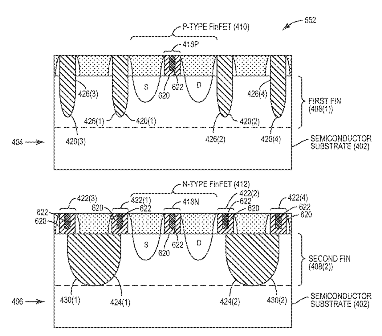
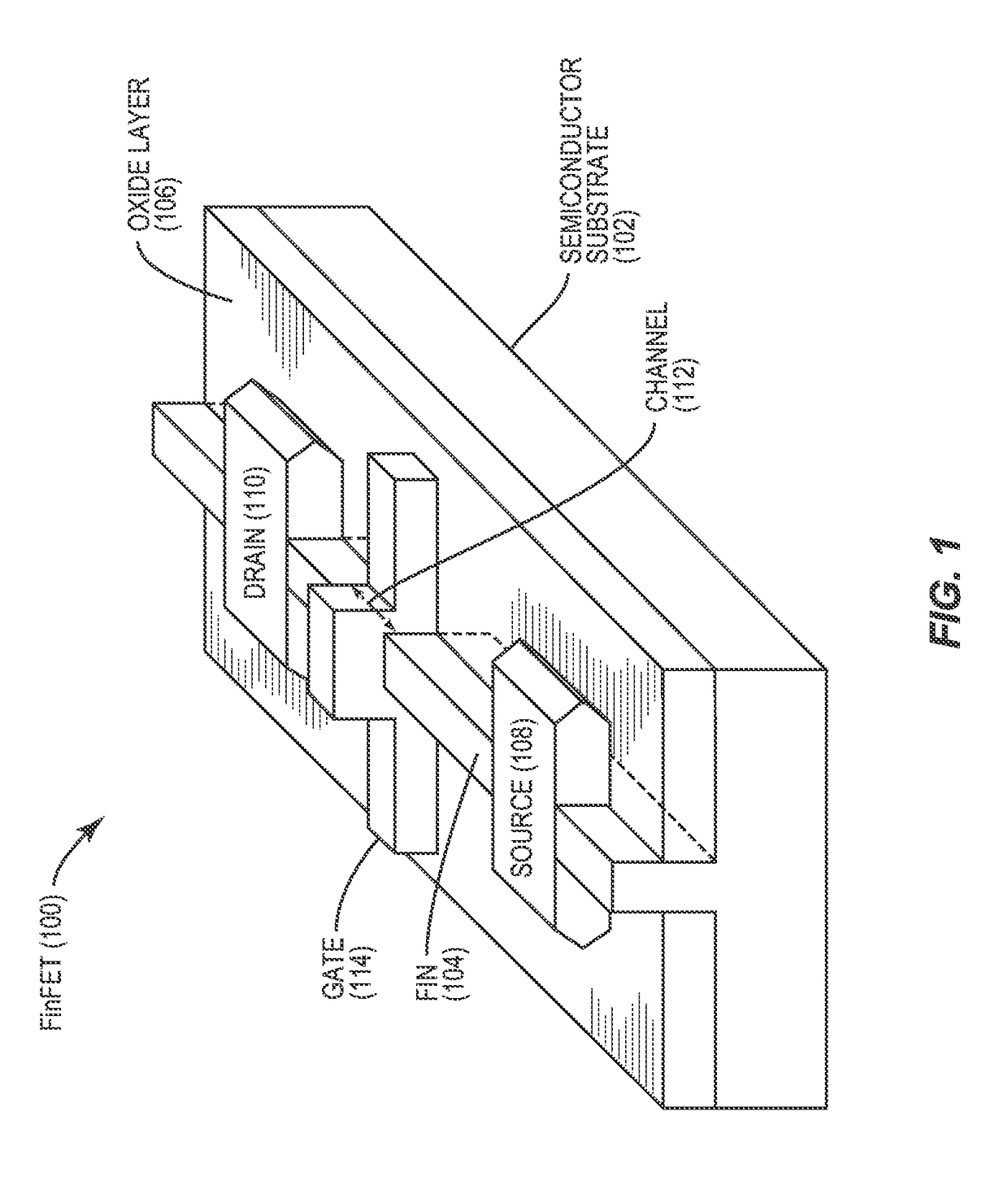
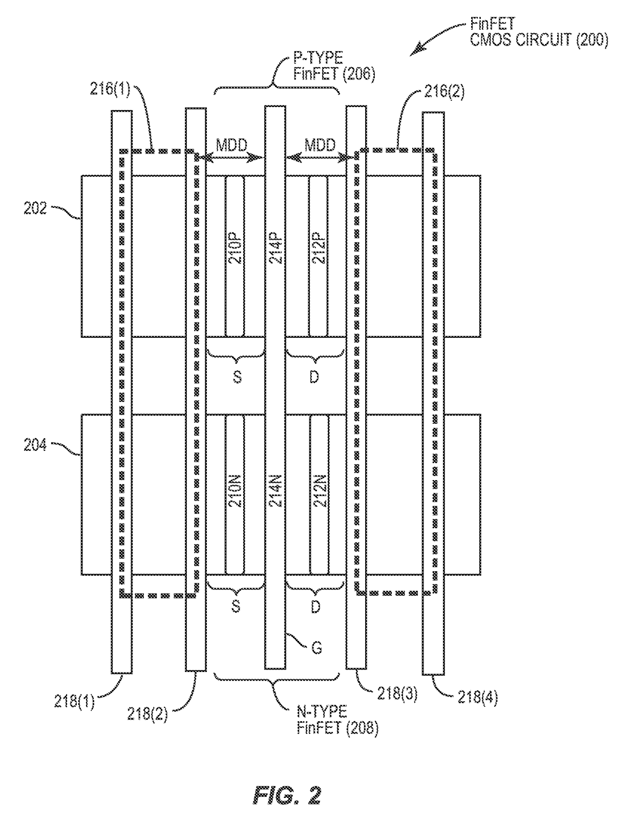
[0022]Aspects disclosed in the detailed description include Fin Field Effect Transistor (FET) (FinFET) complementary metal oxide semiconductor (CMOS) circuits employing single and double diffusion breaks for increased performance. In one aspect, a FinFET CMOS circuit employing single and double diffusion breaks is provided. The FinFET CMOS circuit includes a P-type FinFET that includes a first Fin formed from a semiconductor substrate and corresponding to a P-type semiconductor material (P-type) diffusion region. The FinFET CMOS circuit also includes an N-type FinFET that includes a second Fin formed from the semiconductor substrate and corresponding ...


PUM


Abstract

Fin Field Effect Transistor (FET) (FinFET) complementary metal oxide semiconductor (CMOS) circuits with single and double diffusion breaks for increased performance are disclosed. In one aspect, a FinFET CMOS circuit employing single and double diffusion breaks includes a P-type FinFET that includes a first Fin formed from a semiconductor substrate and corresponding to a P-type diffusion region. The FinFET CMOS circuit includes an N-type FinFET that includes a second Fin formed from the semiconductor substrate and corresponding to an N-type diffusion region. To electrically isolate the P-type FinFET, first and second single diffusion break (SDB) isolation structures are formed in the first Fin on either side of a gate of the P-type FinFET. To electrically isolate the N-type FinFET, first and second double diffusion break (DDB) isolation structures are formed in the second Fin on either side of a gate of the N-type FinFET.

Description

BACKGROUND[0001]I. Field of the Disclosure[0002]The technology of the disclosure relates generally to Fin Field Effect Transistors (FETs) (FinFETs), and particularly to use of diffusion breaks between adjacent elements in FinFET complementary metal oxide semiconductor (CMOS) circuits to improve performance.[0003]II. Background[0004]Transistors are essential components in modern electronic devices. Large numbers of transistors are employed in integrated circuits (ICs) in many modern electronic devices. For example, components such as central processing units (CPUs) and memory systems each employ a large quantity of transistors for logic circuits and memory devices.[0005]As electronic devices become more complex in functionality, so does the need to include a greater number of transistors in such devices. However, as electronic devices are required to be provided in increasingly smaller packages, such as in mobile devices, for example, a greater number of transistors need to be provid...

Claims


Application Information

Patent Timeline
Patent Type & Authority Applications(United States)
IPC IPC(8): H01L27/092H01L29/423H01L29/06H01L21/28H01L21/02H01L21/762H01L21/306H01L29/49H01L21/8238
CPCH01L27/0924H01L29/0649H01L29/42376H01L21/823821H01L21/823878H01L21/823828H01L21/02164H01L21/30604H01L21/28035H01L29/4916H01L21/823814H01L21/76224H01L29/7846H01L21/76232H01L21/762
Inventor YUAN, JUNLIU, YANXIANGRIM, KERN
Owner QUALCOMM INC
Why Eureka
Try Eureka