Surface Defect Inspection With Large Particle Monitoring And Laser Power Control

a technology of large particle and surface defect, applied in semiconductor/solid-state device testing/measurement, instruments, material analysis, etc., can solve the problems affecting the inspection effect, and causing the explosion of large particle size, etc., to achieve the effect of reducing illumination intensity

Active Publication Date: 2018-02-08
KLA TENCOR TECH CORP
View PDF4 Cites 6 Cited by
  • Summary
  • Abstract
  • Description
  • Claims
  • Application Information

AI Technical Summary

Benefits of technology

[0008]Methods and systems for reducing illumination intensity when scanning over large particles are presented herein. A surface inspection system determines the presence of a large particle in the inspe

Problems solved by technology

However, in some examples, high illumination power density causes large size particles to explode due to high power laser heating.
This creates hundreds of smaller particles on the wafer and compounds the contamination problem.
In other examp

Method used


Image

  • Surface Defect Inspection With Large Particle Monitoring And Laser Power Control
  • Surface Defect Inspection With Large Particle Monitoring And Laser Power Control
  • Surface Defect Inspection With Large Particle Monitoring And Laser Power Control

Examples


Embodiment Construction

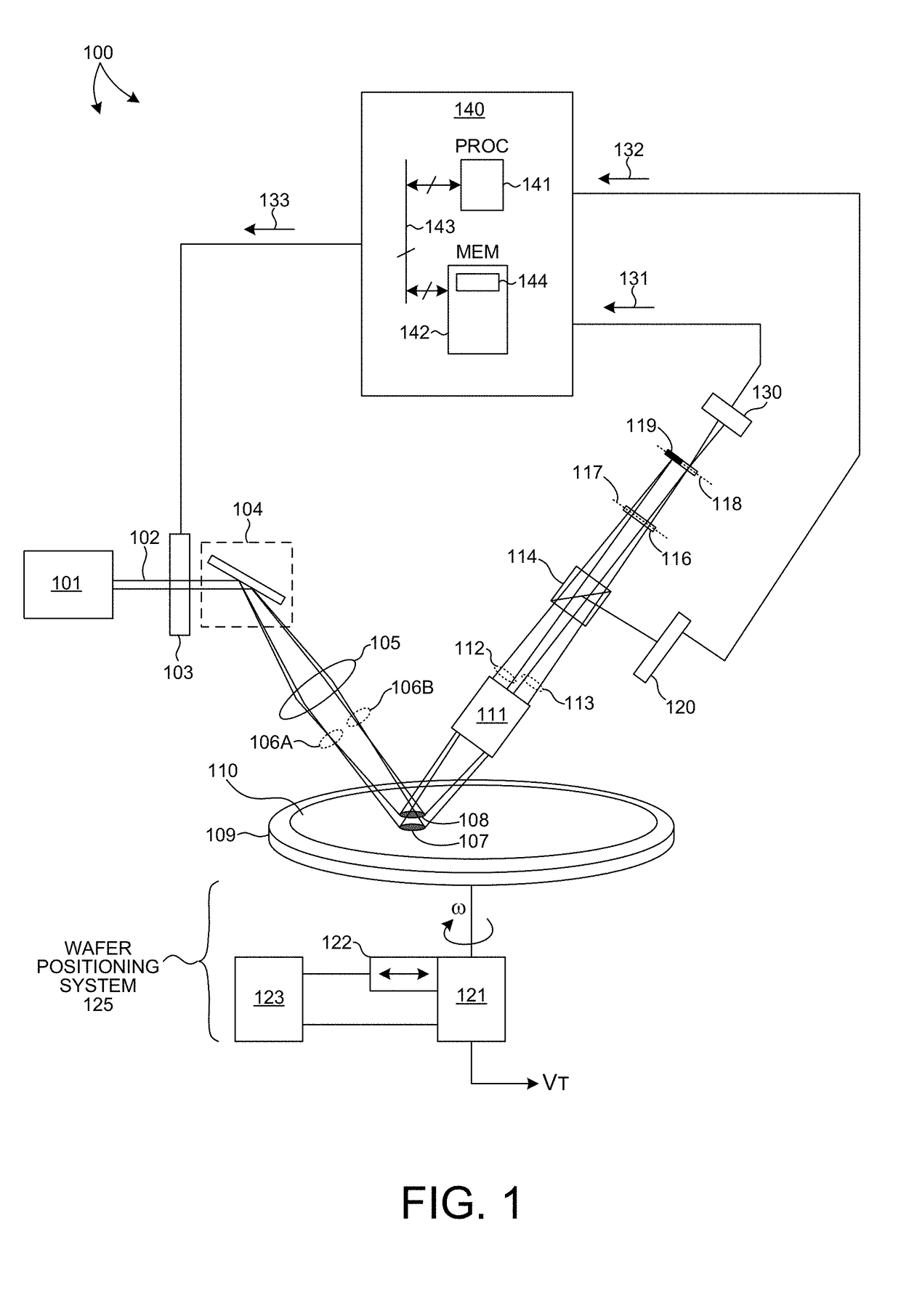
[0029]Reference will now be made in detail to background examples and some embodiments of the invention, examples of which are illustrated in the accompanying drawings.

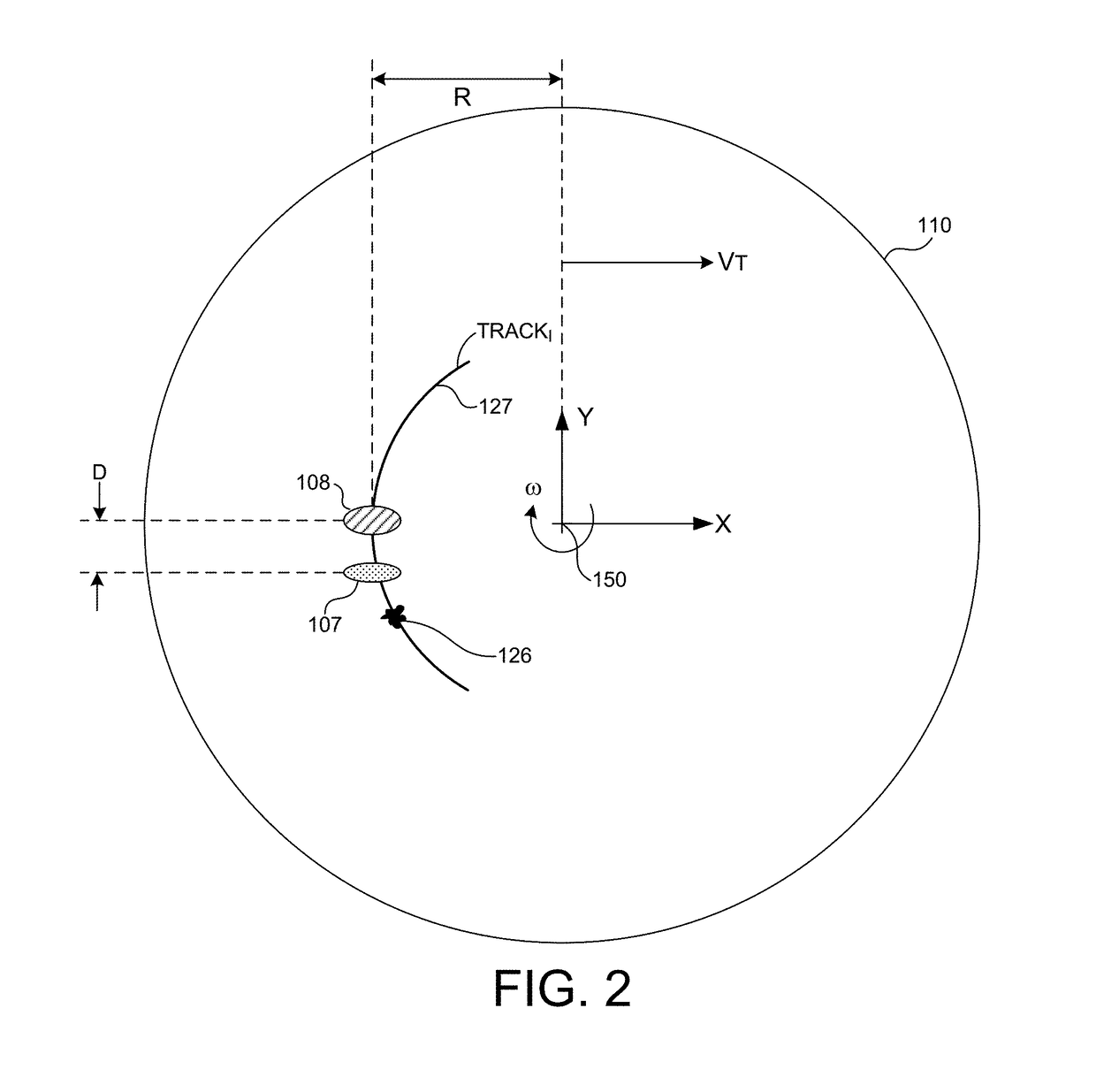
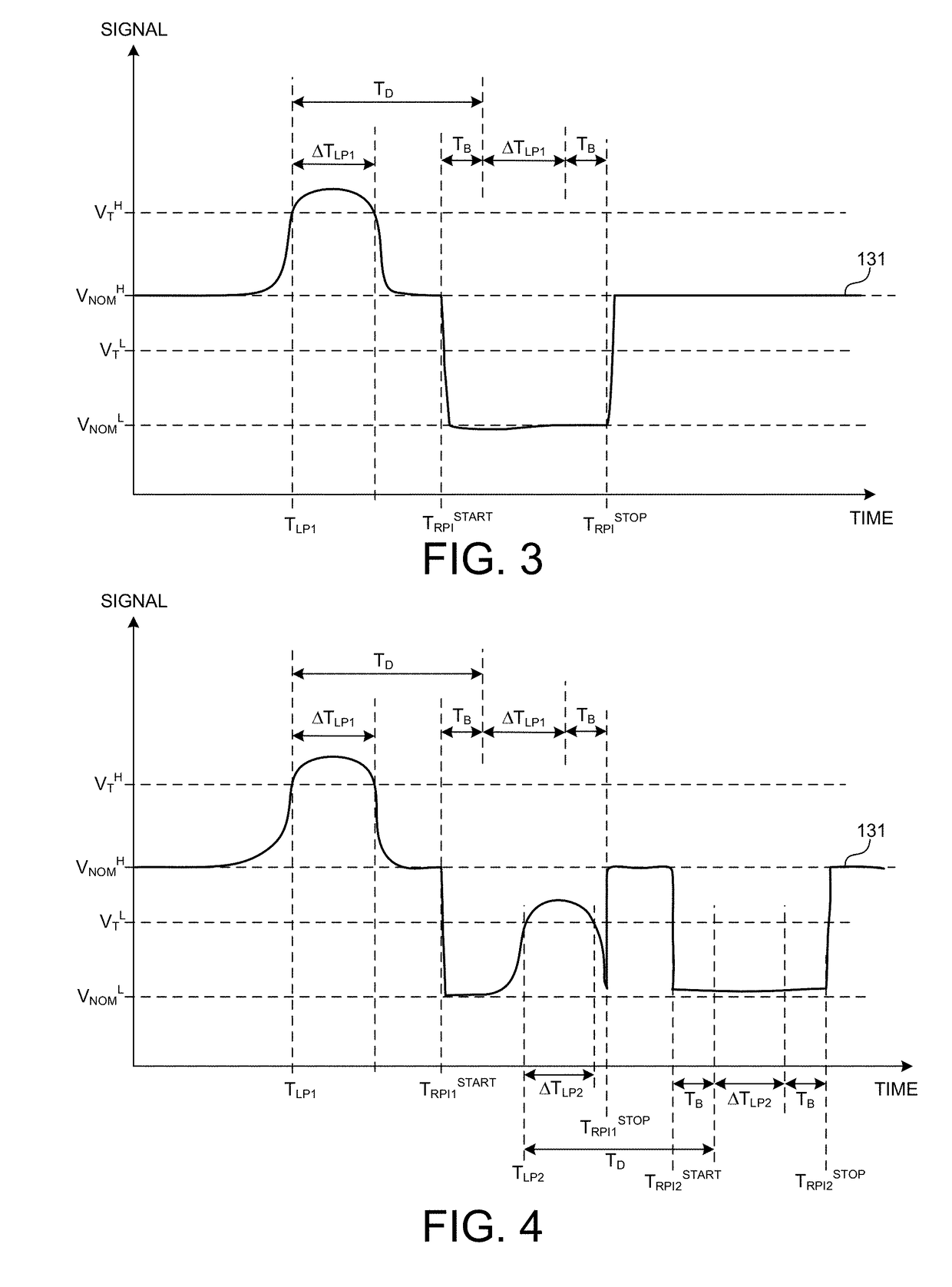
[0030]The inventive concepts described herein are based on the observation that larger particles (e.g., particles greater than one micron in diameter) are more likely to be damaged by the incident laser beam than smaller particles. For example, larger particles have more surface area, and as such, tend to absorb significantly more power than smaller particles having less surface area. Larger particles also tend to scatter significantly more light than smaller particles, due to larger surface area and / or increased surface irregularities. For example, the relative amount of light scattered from a particle of radius, R, is proportional to the particle radius raised to the sixth power. The tendency of large particles to strongly scatter light is exploited to reduce thermal damage during surface inspection.

[0031]In one asp...


PUM


Abstract

Methods and systems for reducing illumination intensity while scanning over large particles are presented herein. A surface inspection system determines the presence of a large particle in the inspection path of a primary measurement spot using a separate leading measurement spot. The inspection system reduces the incident illumination power while the large particle is within the primary measurement spot. The primary measurement spot and the leading measurement spot are separately imaged by a common imaging collection objective onto one or more detectors. The imaging based collection design spatially separates the image of the leading measurement spot from the image of the primary measurement spot at one or more wafer image planes. Light detected from the leading measurement spot is analyzed to determine a reduced power time interval when the optical power of the primary illumination beam and the leading illumination beam are reduced.

Description

TECHNICAL FIELD[0001]The described embodiments relate to systems for surface inspection, and more particularly to semiconductor wafer inspection modalities.BACKGROUND INFORMATION[0002]Semiconductor devices such as logic and memory devices are typically fabricated by a sequence of processing steps applied to a substrate or wafer. The various features and multiple structural levels of the semiconductor devices are formed by these processing steps. For example, lithography among others is one semiconductor fabrication process that involves generating a pattern on a semiconductor wafer. Additional examples of semiconductor fabrication processes include, but are not limited to, chemical-mechanical polishing, etch, deposition, and ion implantation. Multiple semiconductor devices may be fabricated on a single semiconductor wafer and then separated into individual semiconductor devices.[0003]Inspection processes are used at various steps during a semiconductor manufacturing process to detec...

Claims


Application Information

Patent Timeline
IPC IPC(8): G01N21/88G01N21/94G01N21/95
CPCG01N21/8806G01N21/9501G01N2201/06113G01N2021/8835G01N21/94G01N21/956H01L21/67242H01L22/12H01L22/30
Inventor HUANG, CHUNSHENGWANG, CHUNHAIWOLTERS, CHRISTIANWHITESIDE, BRETROMANOVSKY, ANATOLY G.HUANG, CHUANYONGPETTIBONE, DONALD WARREN
Owner KLA TENCOR TECH CORP
Why Eureka
Try Eureka