Radiation detector and radiation detection device using the same

Active Publication Date: 2018-03-01
HITACHI LTD
View PDF9 Cites 3 Cited by
  • Summary
  • Abstract
  • Description
  • Claims
  • Application Information

AI Technical Summary

Benefits of technology

The present invention is a detector that can detect radiation while maintaining strong electric signals in the detector. This is achieved by applying an electric field to the entire inside of the SiC crystal that serves as the detector's layer for detecting radiation. This ensures that the detector can work efficiently and without any reduction in the electric signals generated during operation.

Problems solved by technology

The semiconductor radiation detector detects as an electric signal an electric charge generated by radiation entering a radiation sensible layer, so that noise is involved when the leak electric current flowing as a result of the application of the DC voltage is large.
Thus, it has a problem in that deterioration in detection characteristics is involved.

Method used


Image

  • Radiation detector and radiation detection device using the same
  • Radiation detector and radiation detection device using the same
  • Radiation detector and radiation detection device using the same

Examples


embodiment 1

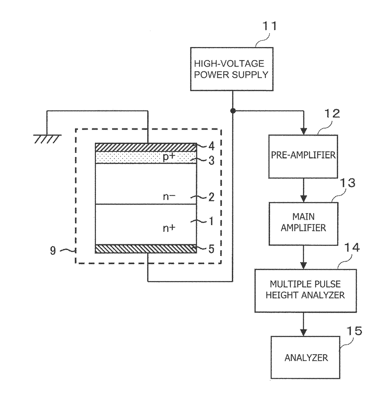
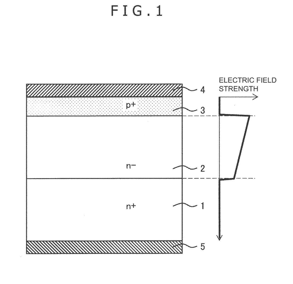
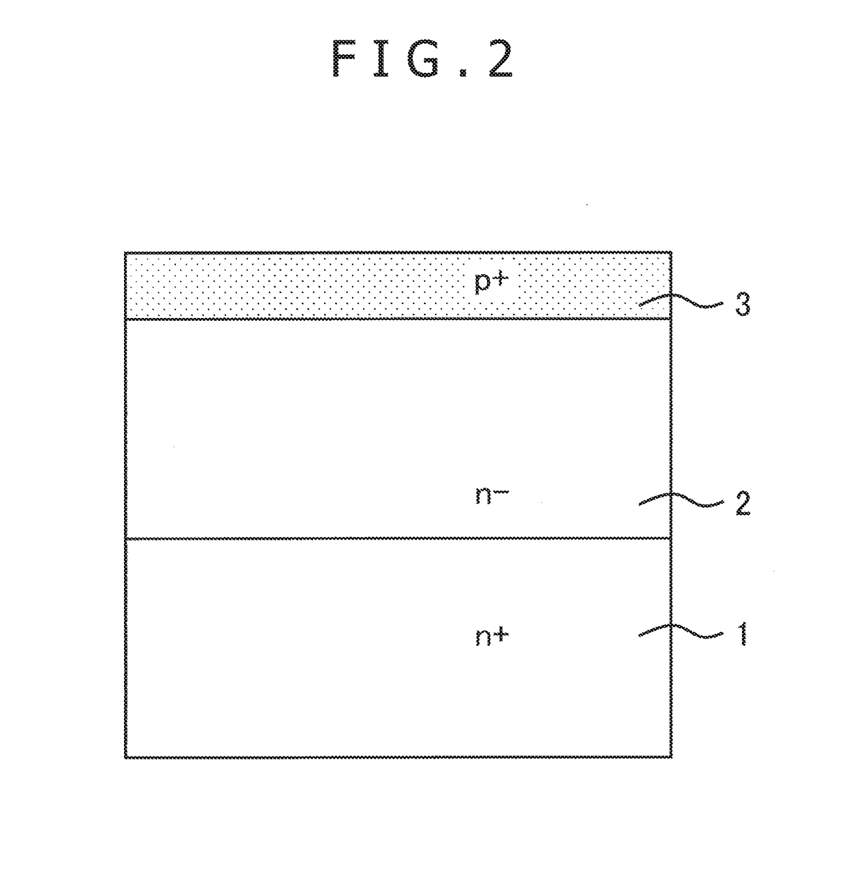
[0023]FIG. 1 is an explanatory view illustrating the sectional structure of a radiation detector according to embodiment 1 of the present invention. The radiation detector according to embodiment 1 is a pn-junction radiation detector equipped with a first conductivity type low impurity concentration (n−) SiC radiation sensible layer 2 formed on a first conductivity type (n-type) high impurity concentration (n+) SiC substrate 1, a second conductivity type (p-type) high impurity concentration (p+) semiconductor region 3, a first electrode 4 provided on the front surface of the p+ semiconductor region 3, and a second electrode 5 provided on the back surface of the n+ SiC substrate 1. Further, in this radiation detector, a higher voltage is applied to the second electrode 5 than to the first electrode 4 during operation, and a depletion layer expands through the entire n− SiC radiation sensible layer 2 in the depth direction, with an electric field being applied thereto.

[0024]FIGS. 2 th...

embodiment 2

[0039]FIG. 8 shows the sectional structure of a radiation detector according to embodiment 2 of the present invention. In embodiment 2, a semi-insulating SiC substrate is employed as the radiation sensible layer.

[0040]This embodiment differs from embodiment 1 shown in FIG. 1 in that the radiation sensible layer is a semi-insulating SiC substrate 7 exhibiting a resistivity of 1×10⁵ Ωcm2 or more and that it has the p+ semiconductor region 3 on the upper surface of the semi-insulating SiC substrate 7, and an n+ semiconductor region 8 on the back surface of the semi-insulating SiC substrate 7. That is, there is prepared an SiC substrate in which the p+ semiconductor region 3 is formed through epitaxial growth on the semi-insulating SiC substrate 7 of a thickness of approximately 100 to 500 μm, and in which the n+ semiconductor region 8 is formed through epitaxial growth on the back surface of the semi-insulating SiC substrate 7. Then, the first electrode 4 is formed on the p+ semiconduc...


PUM


Abstract

There is provided a radiation detector using SiC and of a structure in which an electric field is applied to the interior of the entire SiC crystal constituting a radiation sensible layer, aiming to detect radiation while suppressing a reduction in electric signals generated in the radiation sensible layer.The radiation detector includes: a radiation sensible layer formed of silicon carbide and configured to generate an electron hole pair due to radiation entering it; a first semiconductor region in contact with a first principal surface of the radiation sensible layer and exhibiting a first impurity concentration at least in the region in contact with the radiation sensible layer; a second semiconductor region in contact with a second principal surface on the opposite side of the first principal surface and exhibiting a second impurity concentration at least in the region in contact with the radiation sensible layer; a first electrode connected to the first semiconductor region; and a second electrode connected to the second semiconductor region. The impurity concentration in the radiation sensible layer adjacent to the first semiconductor region, with the first principal surface serving as a border, is discontinuous with the first impurity concentration; the impurity concentration in the radiation sensible layer adjacent to the second semiconductor region, with the second principal surface serving as a border, is discontinuous with the second impurity concentration; and an electric field is applied to the entire radiation sensible layer in the depth direction thereof at a voltage during operation.

Description

TECHNICAL FIELD[0001]The present invention relates to a radiation detector employing silicon carbide.BACKGROUND ART[0002]Regarding a radiation detector capable of energy analysis of incident radiation, there has been mainly employed one consisting of a combination of a scintillator and a photomultiplier tube. In recent years, however, in connection with a radiation detector detecting radiation such as gamma ray, attention is being paid to a semiconductor radiation detection technique according to which a radiation detector is formed by a semiconductor crystal of cadmium telluride (CdTe), gallium arsenide (GaAs) or the like. The semiconductor radiation detector is provided with the semiconductor crystal and electrodes formed on both sides thereof. By applying a DC voltage between the electrodes, an electric charge generated through interaction of the radiation and the semiconductor crystal when radiation such as X-ray or gamma ray enters the semiconductor crystal, is extracted as an ...

Claims


Application Information

Patent Timeline
IPC IPC(8): G01T1/24H01L31/0312H01L31/115H01L31/02H01L31/0224
CPCG01T1/241H01L31/0312H01L31/115H01L31/02019H01L31/022408H01L31/117G01T1/24
Inventor KAMESHIRO, NORIFUMISHIMA, AKIO
Owner HITACHI LTD
Why Eureka
Try Eureka