
Surface-normal optical coupling interface with thermal-optic coefficient compensation

a surface-normal optical coupling and thermal-optic coefficient compensation technology, applied in the direction of optical elements, instruments, semiconductor lasers, etc., can solve the problems of low optical bandwidth, large mismatch in the size of the mode field between silicon waveguides and optical waveguides fabricated with other materials, and achieve the effect of reducing back reflection

Active Publication Date: 2018-04-19
ORACLE INT CORP
View PDF2 Cites 3 Cited by
  • Summary
  • Abstract
  • Description
  • Claims
  • Application Information

AI Technical Summary

Benefits of technology

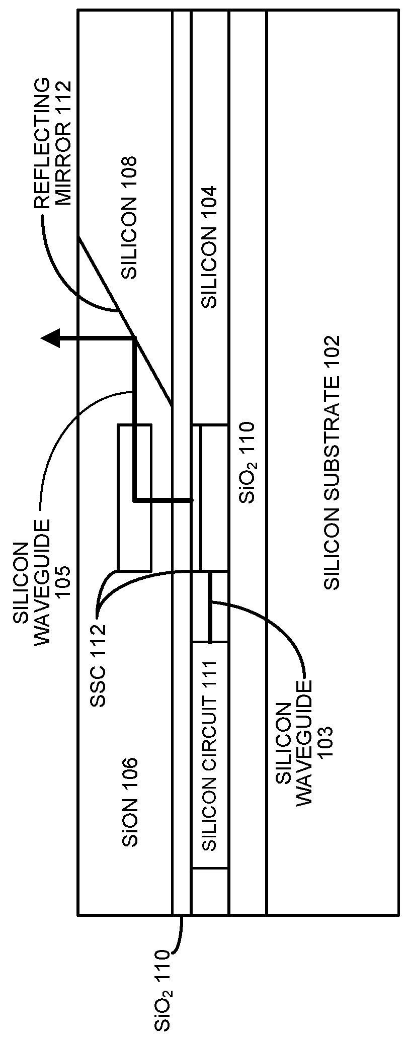
This patent describes a system that includes a component called a spot-size converter (SSC) that increases the size of an optical signal before it exits the semiconductor chip. The system also includes an anti-reflection coating to reduce back reflection, which is applied to the output facet of the chip. These components help improve the quality and accuracy of optical signal transmission in the system.

Problems solved by technology

However, technical challenges arise when light has to be coupled into and out of silicon chips to facilitate off-chip communications.
In particular, there is typically a huge mismatch in the size of the mode field between silicon waveguides and optical waveguides fabricated with other materials, such as optical fibers and III-V semiconductor optical amplifiers (SOAs).
However, this type of coupler suffers from low optical bandwidth, and its polarization-sensitive nature greatly limits its applications when two polarizations are involved.
However, this approach requires very precise control over the vertical alignment between certain materials, such as MN semiconductors and silicon, and it also involves deep etching of a silicon recess area, or substrate thinning of silicon on insulator (SOI), which makes the integration process very complex.
Therefore, this type of coupling does not provide an economical solution for optical packaging.

Method used


Image

  • Surface-normal optical coupling interface with thermal-optic coefficient compensation
  • Surface-normal optical coupling interface with thermal-optic coefficient compensation
  • Surface-normal optical coupling interface with thermal-optic coefficient compensation

Examples


Embodiment Construction

[0025]The following description is presented to enable any person skilled in the art to make and use the present embodiments, and is provided in the context of a particular application and its requirements. Various modifications to the disclosed embodiments will be readily apparent to those skilled in the art, and the general principles defined herein may be applied to other embodiments and applications without departing from the spirit and scope of the present embodiments. Thus, the present embodiments are not limited to the embodiments shown, but are to be accorded the widest scope consistent with the principles and features disclosed herein.

[0026]The data structures and code described in this detailed description are typically stored on a computer-readable storage medium, which may be any device or medium that can store code and / or data for use by a computer system. The computer-readable storage medium includes, but is not limited to, volatile memory, non-volatile memory, magneti...


PUM


Abstract

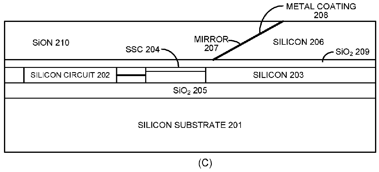
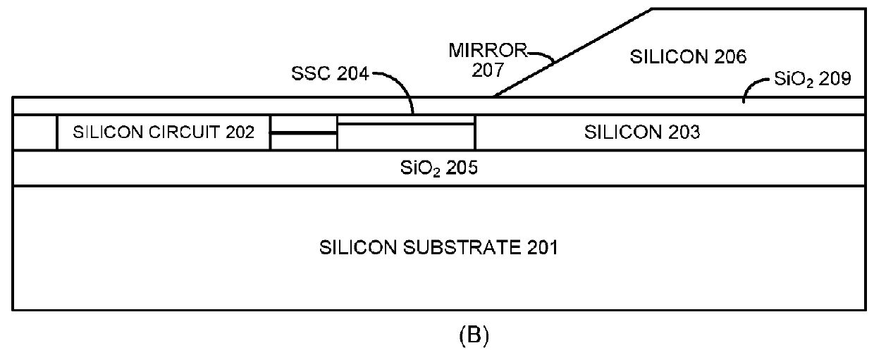
The disclosed embodiments provide a system that implements an optical interface. The system includes a semiconductor chip with a silicon layer, which includes a silicon waveguide, and an interface layer (which can be comprised of SiON) disposed over the silicon layer, wherein the interface layer includes an interface waveguide. The system also includes an optical coupler that couples an optical signal from the silicon waveguide in the silicon layer to the interface waveguide in the interface layer, wherein the interface waveguide channels the optical signal in a direction parallel to a top surface of the semiconductor chip. The system additionally includes a mirror, which is oriented to reflect the optical signal from the interface waveguide in a surface-normal direction so that the optical signal exits the top surface of the semiconductor chip.

Description

GOVERNMENT LICENSE RIGHTS[0001]This invention was made with U.S. government support under Agreement No. HR0011-08-9-0001 awarded by DARPA. The U.S. government has certain rights in the invention.BACKGROUNDField[0002]The disclosed embodiments relate to the design of optical interfaces for silicon-photonic chips. More specifically, the disclosed embodiments relate to the design of a surface-normal optical interface for a silicon-photonic chip that provides thermal-optic coefficient compensation.Related Art[0003]During the past few years, silicon photonics has gained increasing acceptance as a platform of choice for providing photonic integration for short-reach optical communications. At present, a number of useful silicon-photonic devices, such as modulators, detectors and basic passive components, are being fabricated by silicon foundries. However, technical challenges arise when light has to be coupled into and out of silicon chips to facilitate off-chip communications. In particul...

Claims


Application Information

Patent Timeline
IPC IPC(8): G02B6/12H01S5/30H01S5/026H01S5/10G02B6/136G02B6/132
CPCG02B6/12004G02B6/12002H01S5/3013H01S5/026G02B2006/12147G02B6/136G02B6/132G02B2006/12104H01S5/1014G02B6/305H01S3/0813H01S5/021H01S5/02469H01S5/1035H01S5/14H01S5/02326
Inventor LUO, YINGZHENG, XUEZHEKRISHNAMOORTHY, ASHOK V.
Owner ORACLE INT CORP
Learn More