Thin film transistor substrate having bi-layer oxide semiconductor

a thin film transistor and substrate technology, applied in the field of thin film transistor substrates having bi-layer oxide semiconductors, can solve the problems of difficult to drive thin film transistors, poor manufacturing yields (or productivity), and degrade the video quality of the display, and achieve high speed operation, high resistivity, and different composition ratio

Inactive Publication Date: 2018-05-03
LG DISPLAY CO LTD
View PDF4 Cites 11 Cited by
  • Summary
  • Abstract
  • Description
  • Claims
  • Application Information

AI Technical Summary

Benefits of technology

[0028]Accordingly, in order to overcome the above mentioned drawbacks, the present disclosure is to provide an ultra-high definition (UHD) flat panel display over UHD resolution. In addition, the present disclosure is to provide a thin film transistor substrate having short channel length favorable for the high speed operation and with stable threshold voltage for a long time. Further, the present disclosure is to provide a thin film transistor substrate having the superior switching characteristics for large area ultra high density flat panel display.
[0045]The thin film transistor substrate for a flat panel display includes an oxide semiconductor layer having two different type oxide layers. Especially, the upper oxide semiconductor layer at upper layer has different composition ratio from the lower oxide semiconductor layer. As the upper oxide semiconductor layer has higher resistivity than the lower oxide semiconductor layer, the threshold voltage is not changed under the short channel length structure. As the high speed operation can be ensured by the short channel length structure and the stable threshold voltage can be acquired, the present disclosure provides the superior thin film transistor substrate having the stable characteristics under the positive bias stress and / or negative bias stress. The thin film transistor substrate according to the present disclosure provides an ultra high density and large area flat panel display having the superior video quality.

Problems solved by technology

Due to the parasitic capacitance, the video quality of the display can be degraded.
However, when the channel length is too short, the threshold voltage of the thin film transistor can be lowered so that it becomes difficult to drive the thin film transistor.
Since it is difficult to have a thin thickness semiconductor layer over a large area, the manufacturing yields (or productivity) can be very poor.
In this case, due to the doped oxygen particles, the threshold voltage cannot be controlled when the thin film transistor is operated for a long time.

Method used


Image

  • Thin film transistor substrate having bi-layer oxide semiconductor
  • Thin film transistor substrate having bi-layer oxide semiconductor
  • Thin film transistor substrate having bi-layer oxide semiconductor

Examples


Embodiment Construction

[0056]Referring to attached figures, preferred aspects of the present disclosure will be described. Like reference numerals designate like elements throughout the detailed description. However, the present disclosure is not restricted by these aspects but can be applied to various changes or modifications without changing the technical spirit. In the following aspects, the names of the elements are selected for ease of explanation and may be different from actual names.

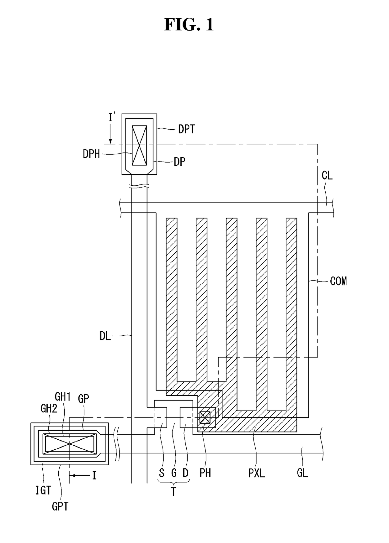
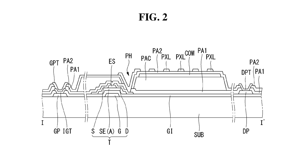
[0057]Hereinafter, we will explain about various structures of a thin film transistor substrate for a flat panel display. Specifically, we will explain as focusing on the structures of a thin film transistor. Applying the thin film transistor substrate including the thin film transistor according to the present disclosure to a display, we can get a flat panel display having the superior video quality.

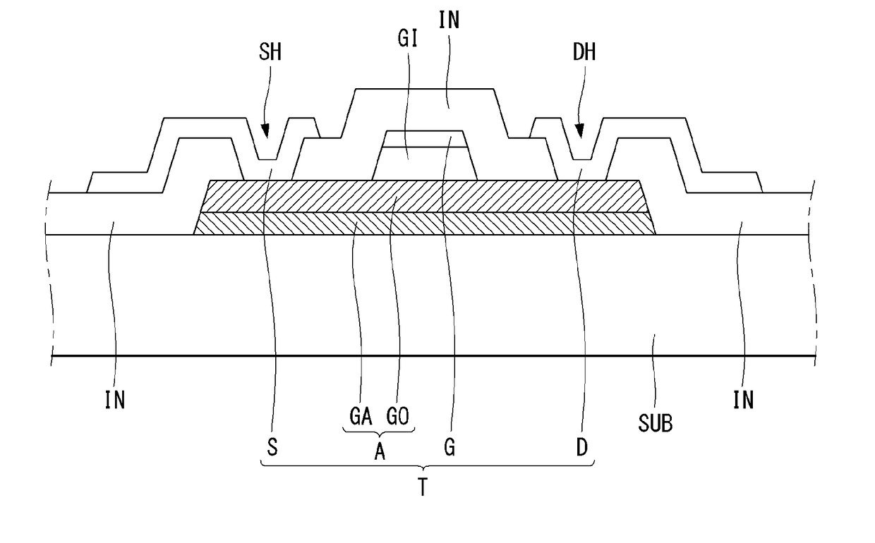
[0058]FIG. 5 is a cross sectional view illustrating a structure of a thin film transistor substrate including an oxide ...


PUM


Abstract

The present disclosure relates to a thin film transistor substrate having a bi-layer oxide semiconductor. The present disclosure provides a thin film transistor substrate comprising: a substrate; and an oxide semiconductor layer on the substrate, wherein the oxide semiconductor layer includes: a first oxide semiconductor layer having indium, gallium and zinc; and a second oxide semiconductor layer stacked on the first oxide semiconductor layer having the indium, gallium and zinc, wherein any one layer of the first and the second oxide semiconductor layers has a first composition ratio of the indium, gallium and zinc of 1:1:1; and wherein other layer has a second composition ratio of the indium, gallium and zinc in which the indium ratio is higher than the zinc ratio.

Description

CROSS-REFERENCE TO RELATED APPLICATION[0001]This application claims priority to Republic of Korea Patent Application Nos. 10-2016-0144008 and 10-2017-0067967, respectively filed on Oct. 31, 2016 and May 31, 2017, which are hereby incorporated by reference in their entirety.BACKGROUNDField of the Disclosure[0002]The present disclosure relates to a display device, and more particularly, to a thin film transistor substrate having a bi-layer oxide semiconductor. Although the present disclosure is suitable for a wide scope of applications, it is particularly suitable for displaying the ultra-high definition (UHD) or higher resolution on the display device.Description of the Background[0003]As the information society is developed, requirements of displays for representing information are increasing. Accordingly, various flat panel displays (or ‘FPD’) are developed for overcoming many drawbacks of the cathode ray tube (or ‘CRT’) such as heavy weight and bulkiness. The flat panel display de...

Claims


Application Information

Patent Timeline
Patent Type & Authority Applications(United States)
IPC IPC(8): H01L27/12H01L29/786H01L29/26H01L29/24
CPCH01L27/1225H01L29/7869H01L29/26H01L29/24H01L27/1222H01L29/78696
Inventor LEE, SOHYUNGKIM, SUNGKIYI, YOUNGJINKIM, MINCHEOLYANG, JEONGSUKIM, SEOYEON
Owner LG DISPLAY CO LTD
Why Eureka
Try Eureka