Ring-type field effect transistor for terahertz wave detection, which uses gate metal as antenna

a field effect transistor and gate metal technology, applied in the direction of antennas, antenna details, semiconductor devices, etc., can solve the problems of difficult integration of peripheral elements such as antennas and amplifiers, difficulty in applying various asymmetric structures, and high manufacturing costs of silicon

Active Publication Date: 2018-05-03
UNIST ULSAN NAT INST OF SCI & TECH
View PDF0 Cites 3 Cited by
  • Summary
  • Abstract
  • Description
  • Claims
  • Application Information

AI Technical Summary

Benefits of technology

[0017]According to an aspect of the present invention, it is possible to provide a ring-type field-effect transistor (FET) for detecting a terahertz wave using a gate metal as an antenna, the ring-type FET which forms a channel to encompass a source in order to obtain an asymmetry based on a geometric form, additionally obtains the asymmetry by adjusting an overlap area between the channel and a gate and an overlapping area between the gate and the source, freely sets each parameter for defining a shape, and uses a metal gate as an antenna without need to employ an antenna as an additional element, so as to implement a high-degree of integration.

Problems solved by technology

However, in terms of the compound semiconductors, a manufacturing cost may be higher than that of the silicon and, due to an inconvenience in an etching process for forming a shape, it is difficult to apply various asymmetric structures.
Also, when using the compound semiconductors, an integration of peripheral elements such as an antenna and an amplifier may be difficult.
For this reason, a commercialization of the compound semiconductor may also be difficult.
Basically, since the silicon FET has a low power characteristic, the improvement of the reactivity of the terahertz detector may be limited when the performances of the peripheral elements are improved only.
Even if the aforementioned scheme is used, the output voltage of the FET that is based on a symmetric structure may be susceptible to noise and thus, a degree of improvement of the reactivity may be relatively small.
Also, an additional complex mask process such as an ion implantation process of overlapping for ultrafine and high-performance elements may be required to change either the source / drain areas overlapping the gate.
In an underlap structure, the asymmetry effect of the gate following a generation of the underlap may be insignificant and a resistance of an element may increase, which may lead to an increase in noise equivalent power.

Method used


Image

  • Ring-type field effect transistor for terahertz wave detection, which uses gate metal as antenna
  • Ring-type field effect transistor for terahertz wave detection, which uses gate metal as antenna
  • Ring-type field effect transistor for terahertz wave detection, which uses gate metal as antenna

Examples


Embodiment Construction

[0022]Reference will now be made in detail to embodiments of the present invention, examples of which are illustrated in the accompanying drawings, wherein like reference numerals refer to the like elements throughout.

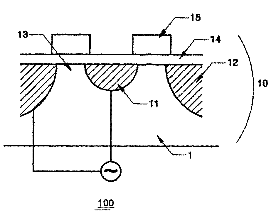
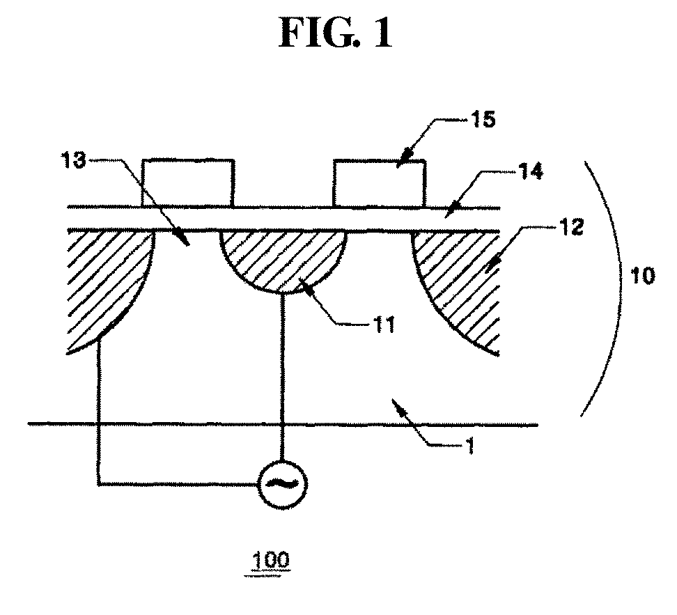
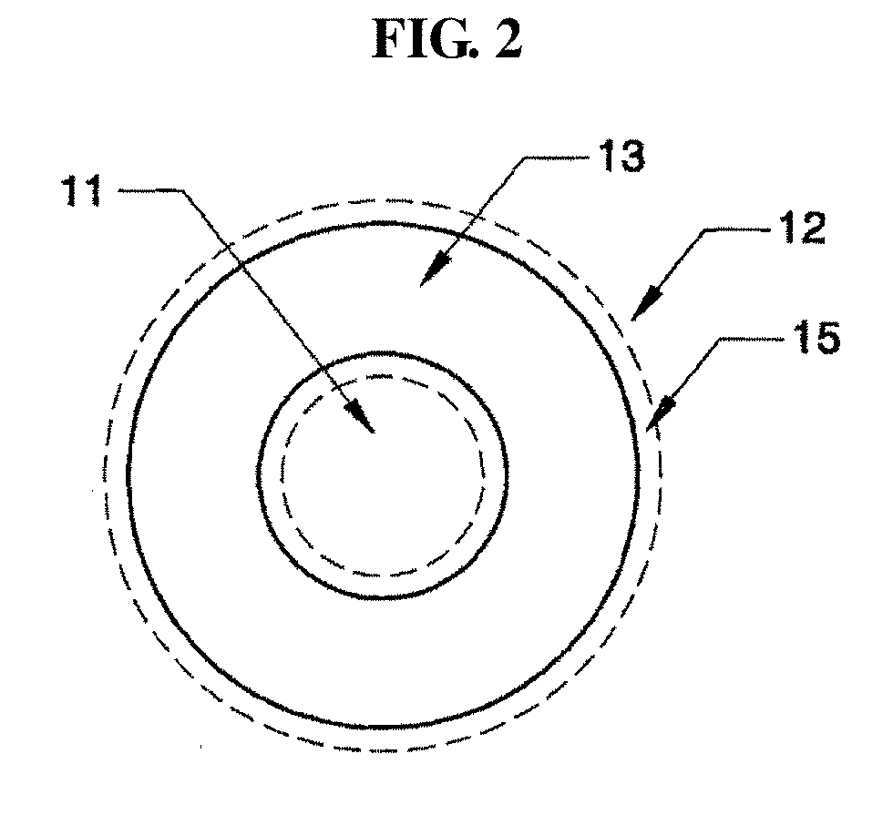
[0023]Referring to FIG. 1, a ring-type field-effect transistor (FET) 10 for detecting a terahertz wave using a gate metal as an antenna may include a source 11, a drain 12, a channel 13, a dielectric layer 14, and a gate 15 formed on a silicon base 1. Hereinafter, the ring-type FET 10 is also referred to as an FET 10.

[0024]An impurity may be doped into each of the source 11 and the drain 12. The dielectric layer 14 may be formed of a material generally applicable to an FET. The gate 15 may be formed of a metal to function as an antenna.

[0025]A terahertz electromagnetic wave may be applied to the gate 13. In this instance, a property of the terahertz electromagnetic wave applied by a voltage generated between the source 11 and the drain 12 may be detected.

[0026]Dependin...


PUM


Abstract

A ring-type FET may include a silicon base, a source formed on a portion of the silicon base through doping, a channel formed to encompass the source on a plane, a drain formed outside the channel, a dielectric layer formed on the source, the channel and the drain, and a gate provided on the dielectric layer, wherein a center of the source is spaced apart from a center of the channel, and the gate is formed of a metal material, disposed above the channel and configured to cover an upper face of the channel and overlap a portion of the source and a portion of the drain.

Description

TECHNICAL FIELD[0001]The present invention relates to a ring-type field-effect transistor (FET) for detecting a terahertz wave using a gate metal as an antenna and, more particularly, to a ring-type FET for detecting a terahertz wave using a gate metal that maximizes an asymmetric effect as an antenna.BACKGROUND ART[0002]To increase a sensitivity in a terahertz detector, a charge of a channel may be gathered in a two-dimensional (2D) form by a gate field effect. In general, compound semiconductors have a relatively high efficiency of forming a 2D channel charge as compared to silicon and thus, have been widely used. However, in terms of the compound semiconductors, a manufacturing cost may be higher than that of the silicon and, due to an inconvenience in an etching process for forming a shape, it is difficult to apply various asymmetric structures. Also, when using the compound semiconductors, an integration of peripheral elements such as an antenna and an amplifier may be difficul...

Claims


Application Information

Patent Timeline
Patent Type & Authority Applications(United States)
IPC IPC(8): H01L29/417H01L29/423H01L29/10H01L29/08H01L31/112H01L29/78
CPCH01L29/41758H01L29/4238H01L29/1033H01L29/0847H01L29/42376H01L31/1126H01L29/78H01Q1/2283
Inventor KIM, KYUNG ROKRYU, MIN WOOAHN, SANG HYO
Owner UNIST ULSAN NAT INST OF SCI & TECH
Why Eureka
Try Eureka