Fabrication method of electronic package having embedded package block

a technology of electronic packages and package blocks, applied in the field of packaging processes, can solve the problems of increasing the number of fabrication steps and the fabrication cost, adversely affecting the quality of the circuit structure, and the laser drilling process is quite slow and time-consuming, so as to improve the electrical transmission performance of the conductive posts, improve the reliability of the electronic package, and save the fabrication time

Active Publication Date: 2018-06-07
SILICONWARE PRECISION IND CO LTD
View PDF2 Cites 2 Cited by
  • Summary
  • Abstract
  • Description
  • Claims
  • Application Information

AI Technical Summary

Benefits of technology

[0025]According to the present invention, the package block having the conductive post are fabricated first and then the encapsulant is formed to encapsulate the package block. As such, the present invention dispenses with the conventional processes for forming the conductive post in the encapsulant, for example, a laser drilling process for forming through holes in the encapsulant, a cleaning process for cleaning the through holes, and an electroplating process for filling the through holes with a conductive material. Therefore, the present invention saves the fabrication time, improves the electrical transmission performance of the conductive posts and avoids the conventional drawback of delamination of the conductive posts from uneven wall surfaces of the through holes, thereby improving the reliability of the electronic package.
[0026]Further, by dispensing with the laser drilling process, the present invention avoids formation of a heat affected zone and hence allows the conductive posts or the package block to be positioned close to the electronic element according to the practical need. Therefore, the size of the electronic package can be reduced to meet the miniaturization requirement.

Problems solved by technology

However, the laser drilling process for forming the through holes 130 can easily destroy the copper foil 120 and consequently adversely affect the quality of the circuit structure 16.
Further, the laser drilling process is quite slow and time-consuming, especially when the number of the through holes is large.
Accordingly, a cleaning process is required before filling of the conductive material in the through holes 130, thus increasing the number of fabrication steps and the fabrication cost.
In addition, if the through holes 130 have a high aspect ratio, it will become difficult to completely remove the residue in the through holes 130.
As such, the electrical transmission performance of the conductive posts 14 may be adversely affected by the remaining residue.
Further, the laser drilling process results in uneven wall surfaces of the through holes 130.
As such, during a subsequent electroplating process, the conductive material cannot be effectively attached to the wall surfaces of the through holes 130 and easily delaminates therefrom, thus reducing the product reliability of the semiconductor package 1.

Method used


Image

  • Fabrication method of electronic package having embedded package block
  • Fabrication method of electronic package having embedded package block
  • Fabrication method of electronic package having embedded package block

Examples


Embodiment Construction

[0030]The following illustrative embodiments are provided to illustrate the disclosure of the present invention, these and other advantages and effects can be apparent to those in the art after reading this specification.

[0031]It should be noted that all the drawings are not intended to limit the present invention. Various modifications and variations can be made without departing from the spirit of the present invention. Further, terms such as “first”, “second”, “on”, “a” etc. are merely for illustrative purposes and should not be construed to limit the scope of the present invention.

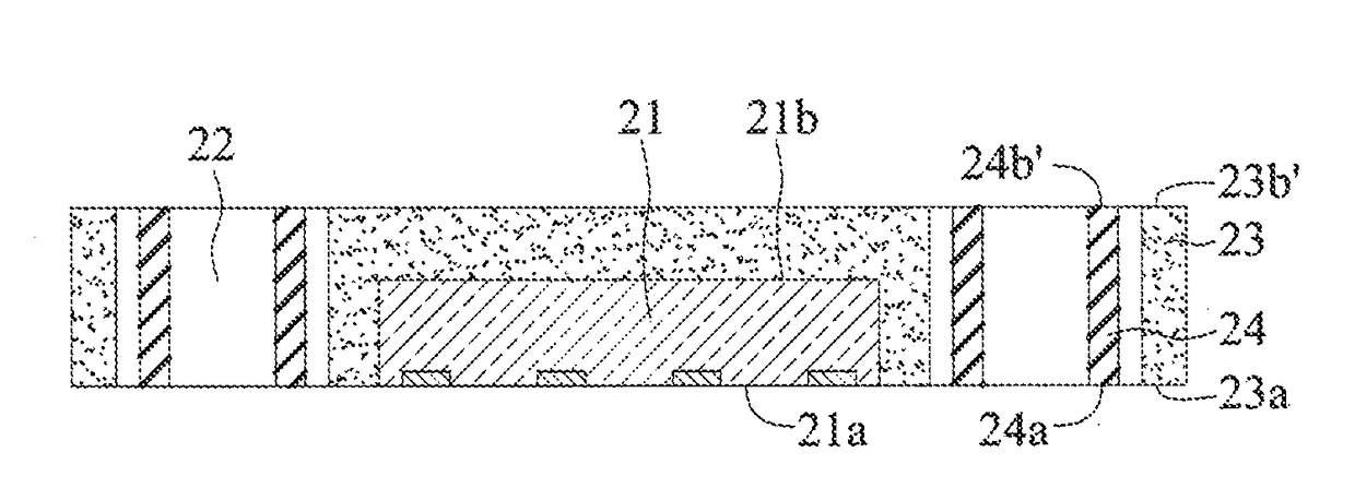
[0032]FIGS. 2A to 2G are schematic cross-sectional views showing a method for fabricating an electronic package 2 according to the present invention.

[0033]Referring to FIG. 2A, a metal board 24′ having a plurality of conductive posts 24 thereon is provided.

[0034]In the present embodiment, the metal board 24′ and the conductive posts 24 are integrally formed. For example, a copper substrate is patterned...


PUM


Abstract

A method for fabricating an electronic package is provided, including steps of: providing a carrier having at least an electronic element and at least a package block disposed thereon, wherein the package block has a plurality of conductive posts bonded to the carrier; forming an encapsulant on the carrier for encapsulating the electronic element and the package block; and removing the carrier so as to expose the electronic element and the conductive posts from a surface of the encapsulant. As such, the invention dispenses with formation of through holes in the encapsulant for forming the conductive posts as in the prior art, thereby saving the fabrication cost.

Description

CROSS-REFERENCE TO RELATED APPLICATION(S)[0001]This application is a divisional of copending application U.S. Ser. No. 14 / 983,049, filed on Dec. 29, 2015, which claims under 35 U.S.C. §119(a) the benefit of Taiwanese Application No. 104130064, filed Sep. 11, 2015, the entire contents of which are incorporated herein by reference.BACKGROUND OF THE INVENTION1. Field of the Invention[0002]The present invention relates to packaging processes, and more particularly, to an electronic package having an electronic element embedded therein and a fabrication method thereof.2. Description of Related Art[0003]Along with the progress of semiconductor packaging technologies, various package types have been developed for semiconductor devices. To improve electrical performance and save space, a plurality of packages can be stacked to form a package on package (PoP) structure, for example, a fan out package on package (FO PoP) structure, thereby greatly increasing I / O count and integrating integrat...

Claims


Application Information

Patent Timeline
Patent Type & Authority Applications(United States)
IPC IPC(8): H01L23/552H01L25/10H01L25/00H01L23/31H01L21/56H01L23/00
CPCH01L21/561H01L25/105H01L2924/18162H01L2924/19041H01L2924/19042H01L2924/19043H01L23/3128H01L21/568H01L23/552H01L24/19H01L24/20H01L24/96H01L2224/24137H01L21/56H01L23/31H01L2225/1058H01L2225/1041H01L2225/1035H01L2224/73267H01L2224/73265H01L2224/48227H01L2224/48091H01L2224/32225H01L2224/16227H01L2224/12105H01L2924/15311H01L25/50H01L2224/04105H01L2224/2518H01L2924/00014H01L2924/00012H01L2924/00
Inventor LEE, MENG-TSUNGHUANG, FU-TANG
Owner SILICONWARE PRECISION IND CO LTD
Why Eureka
Try Eureka