Printed wiring board, printed circuit board, and electronic apparatus

a printed circuit board and wiring board technology, applied in the direction of printed circuit aspects, cross-talk/noise/interference reduction, semiconductor/solid-state device details, etc., can solve the problems of power supply noise, malfunction, and large variation in the propagation time of electric signals, and achieve small inductance

Active Publication Date: 2018-06-14
CANON KK
View PDF4 Cites 13 Cited by
  • Summary
  • Abstract
  • Description
  • Claims
  • Application Information

AI Technical Summary

Benefits of technology

[0006]Therefore, it is an object of the present invention to provide a printed wiring board, a printed circuit board, and an electronic apparatus having a power supply wiring structure of which occupied area is small and which has a small inductance.

Problems solved by technology

Higher data transfer speed results in a greater variation in the propagation times of the electric signals due to various noises.
In the clock synchronous type interface, as the jitter increases, the timing margin decreases, so that a malfunction tends to occur.
One of the causes of jitter is power supply noise.
When the switching current flows in the parasitic inductance, a counter electromotive force is generated, and this counter electromotive force becomes power supply noise.
The power supply noise changes the drive voltage of the buffer circuit, and the output timing of the signal from the buffer circuit fluctuates.
However, when the occupied area is increased by increasing the numbers of power supply vias, ground vias and the like, a parasitic inductance is generated by an increase in the wiring, so that there is a limitation on the reduction of the inductance by such method.

Method used


Image

  • Printed wiring board, printed circuit board, and electronic  apparatus
  • Printed wiring board, printed circuit board, and electronic  apparatus
  • Printed wiring board, printed circuit board, and electronic  apparatus

Examples


first embodiment

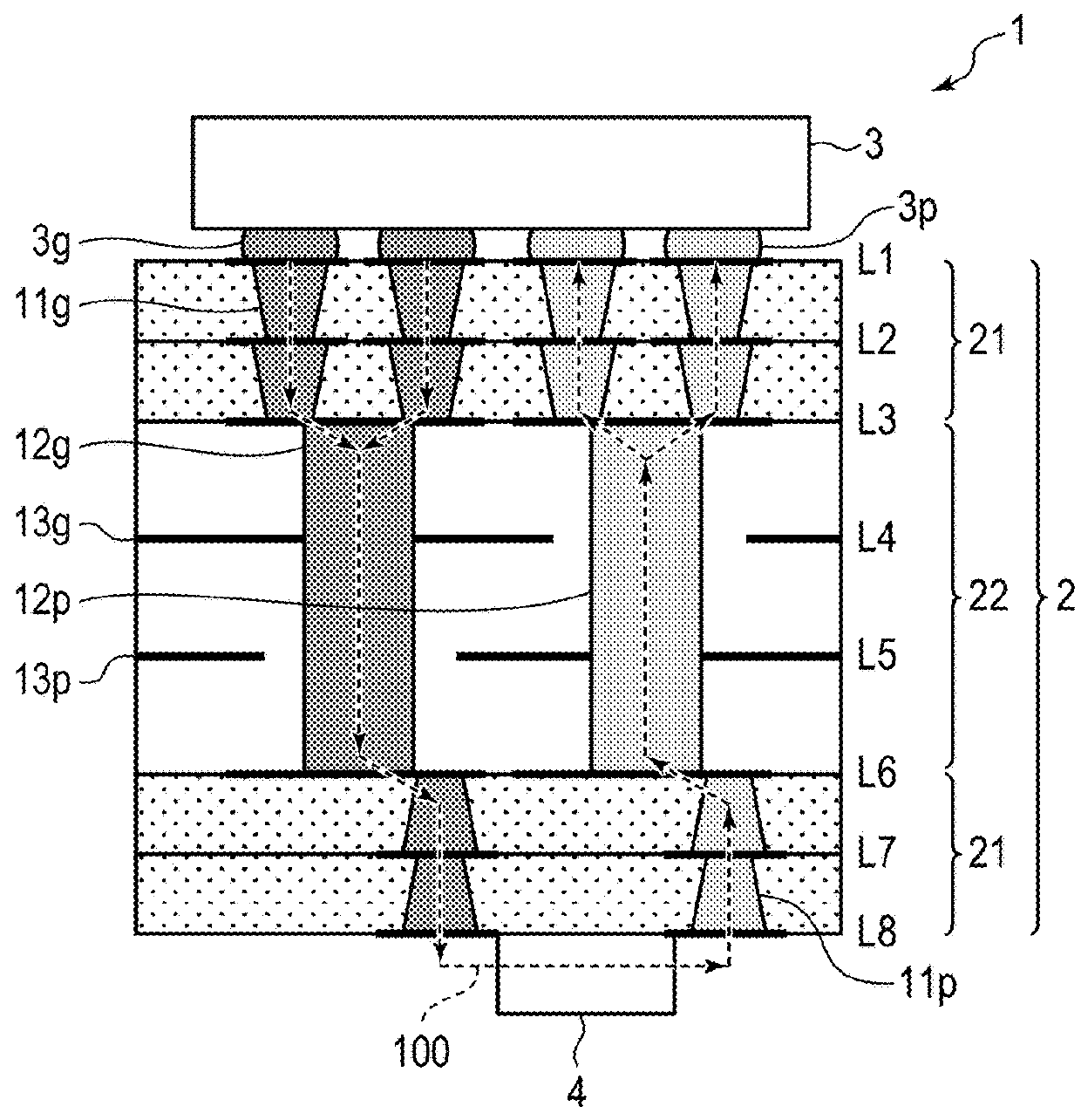
[0022]FIG. 1 is a cross sectional view illustrating a printed circuit board 1 according to a first embodiment. As illustrated in FIG. 1, the printed circuit board 1 includes a printed wiring board 2, a semiconductor device3, and a capacitor 4 serving as a bypass device. The semiconductor device 3 includes a power supply terminal 3p, a ground terminal 3g, and a signal terminal (not shown). Each terminal of the semiconductor device 3 has a structure of Ball Grid Array (BGA), and the semiconductor device 3 can be mounted on the printed wiring board 2 by soldering. The capacitor 4 is a surface mount device having two external electrode terminals capable of being surface-mounted, and can be mounted on the printed wiring board 2 by soldering.

[0023]The printed wiring board 2 is a build-up wiring board with a core layer 22 and build-up layers 21 formed on both sides of the core layer 22. Each build-up layer 21 has a power supply build-up via 11p and a ground build-up via 11g. The core layer...

second embodiment

[0066]Subsequently, in the second embodiment of the present invention, the power supply structure of the printed wiring board 2a in which the power supply core vias 12p and the ground core vias 12g constituting the parallel hexagon 103 shown in the first embodiment are repeatedly arranged in the plane direction will be explained. In each figure, only three cycles of the repetitive arrangement are shown, but the number of cycles can be changed.

[0067]FIG. 5 is a sectional view illustrating a printed circuit board 1a according to the second embodiment. As shown in FIG. 5, the printed circuit board 1a has a printed wiring board 2a, a semiconductor device 3, and a plurality of capacitors 4 which are bypass devices. The configuration of FIG. 5 is similar to that of FIG. 1 except that the structures of the vias shown in FIG. 1 are repeatedly arranged. Therefore, a detailed description thereabout is omitted.

[0068]FIG. 6A to FIG. 6E are plan views illustrating the wiring layers constituting ...

third embodiment

[0075]Subsequently, in the third embodiment of the present invention, a method of arranging the corner portion when the power supply core vias 12p and the ground core vias 12g are repeatedly arranged in the plane direction will be explained. Since the third embodiment of the present invention is the same as the second embodiment except for the vicinity of the corner portion, repeated explanation may be omitted. For example, the sectional structure of the printed wiring board 2a is the same as that of the second embodiment. Therefore, illustration and description thereabout are omitted. In each figure, only four cycles of the repetitive arrangement are shown, but the number of cycles can be changed.

[0076]FIG. 8A is a plan view of the wiring layer L1 of the printed wiring board 2a. The surface layer power supply pad 10p, the surface layer ground pad 10g, and the like are arranged line-symmetrically with respect to the straight line 106. More specifically, in the area A on the upper le...


PUM


Abstract

Provided is a printed wiring board including: a plurality of inner layers including a ground layer and a power supply layer; and a plurality of ground vias and a plurality of power supply vias each provided to penetrate at least the ground layer and the power supply layer in a thickness direction of the printed wiring board, a ground potential being applied to the plurality of ground vias at the ground layer, and a power supply potential being applied to the plurality of power supply vias at the power supply layer. In a top view from a direction perpendicular to the printed wiring board, a distance between vias to which the same potential is applied is shorter than a distance between vias to which different potentials are applied.

Description

BACKGROUND OF THE INVENTIONField of the Invention[0001]The present invention relates to a printed wiring board, a printed circuit board, and an electronic apparatus.Description of the Related Art[0002]As electronic apparatus achieves higher functionality and higher performance, the data transfer speed between semiconductor devices mounted on the printed wiring board has increased. Higher data transfer speed results in a greater variation in the propagation times of the electric signals due to various noises. This variation in the propagation time is called jitter. In the clock synchronous type interface, as the jitter increases, the timing margin decreases, so that a malfunction tends to occur. An example of an electronic apparatus that uses such a clock synchronous interface includes a Double-Data-Rate4 Synchronous Dynamic Random Access Memory.[0003]One of the causes of jitter is power supply noise. As an example of jitter caused by power supply noise, there is simultaneous switchi...

Claims


Application Information

Patent Timeline
Patent Type & Authority Applications(United States)
IPC IPC(8): H05K1/11H01L23/48H05K1/02
CPCH01L23/48H05K1/0218H05K1/115H05K1/0216H05K2201/09318H05K2201/09609H05K2201/09627H01L2224/16225H01L23/49822H01L23/49827H01L23/49838H01L23/50
Inventor NUMAGI, TAKASHITAZAWA, YOUHEIMATSUMOTO, SHOJI
Owner CANON KK
Why Eureka
Try Eureka