Method and Apparatus for Defect Inspection of Transparent Substrate

a transparent substrate and defect technology, applied in the direction of instruments, measurement devices, holographic optical components, etc., can solve the problems of easy loss of focus or without focusing, and the method is not suitable for the detection of micro-bubble defects on glass,

Active Publication Date: 2018-07-05
NATIONAL TAIWAN NORMAL UNIVERSITY
View PDF6 Cites 12 Cited by
  • Summary
  • Abstract
  • Description
  • Claims
  • Application Information

AI Technical Summary

Problems solved by technology

However, in the disclosure of the above-mentioned patent applications, method of detection and classification of defects on glass only performs edge detection for the image to obtain edge information of the defects.
Such methods are not suitable for detection of micro bubble defects on glass, and the micro bubble detection system or device is still needed to be further improved for facilitating detection of the defects.
However, through the machine vision camera, only the intensity image can be obtained, and the complex images information of the glass substrate can't be obtained completely.
Furthermore, it is easy to lose focus or without focusing because the camera can't effectively focus on transparent substrate.
Therefore, it is often necessary to carry out a complicated and time-consuming algorithm for multiple pre-signal processing and classification to proceed the following detection task.
Thus, the existing machine vision can't provide quickly and effectively detect the transparent substrate and improve yield of detection due to the above complicated operations.
However, in the wide-field optical imaging system of traditional defect detection, some problems exist, such as: poor image pixel resolution of sensor, that require the use of mechanical scanning and image stitching and other related technologies, to complete wide field reconstructed image with high resolution of a large area.
This leads to time-consuming of defect detection process, so that only some samples can be extracted to shorten the detection time.
In addition, the defect detection technology of traditional industrial products can't be applied to penetrating detection of transparent glass substrate.
Therefore, how to effectively implement the detection of transparent substrate to improve resolution and field of view, and shorten the detecting time and improve the detection area, has become an important issue in the industry and field of detection.
Therefore, how to improve the field of view and high resolution imaging mechanism to shorten the detection time and increase the number of detection has become an important issue in the current defect detection.
The defects of the transparent substrate may lead to serious yield decline of the whole product process and assembly, and greatly increase the cost of production and waste of resources.
However, at present, there is no effective and reliable transparent substrate defect detection technology and method available for industrial applications.

Method used


Image

  • Method and Apparatus for Defect Inspection of Transparent Substrate
  • Method and Apparatus for Defect Inspection of Transparent Substrate
  • Method and Apparatus for Defect Inspection of Transparent Substrate

Examples


Embodiment Construction

[0051]Some preferred embodiments of the present invention will now be described in greater detail. However, it should be recognized that the preferred embodiments of the present invention are provided for illustration rather than limiting the present invention. In addition, the present invention can be practiced in a wide range of other embodiments besides those explicitly described, and the scope of the present invention is not expressly limited except as specified in the accompanying claims.

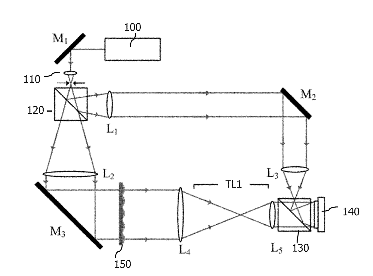
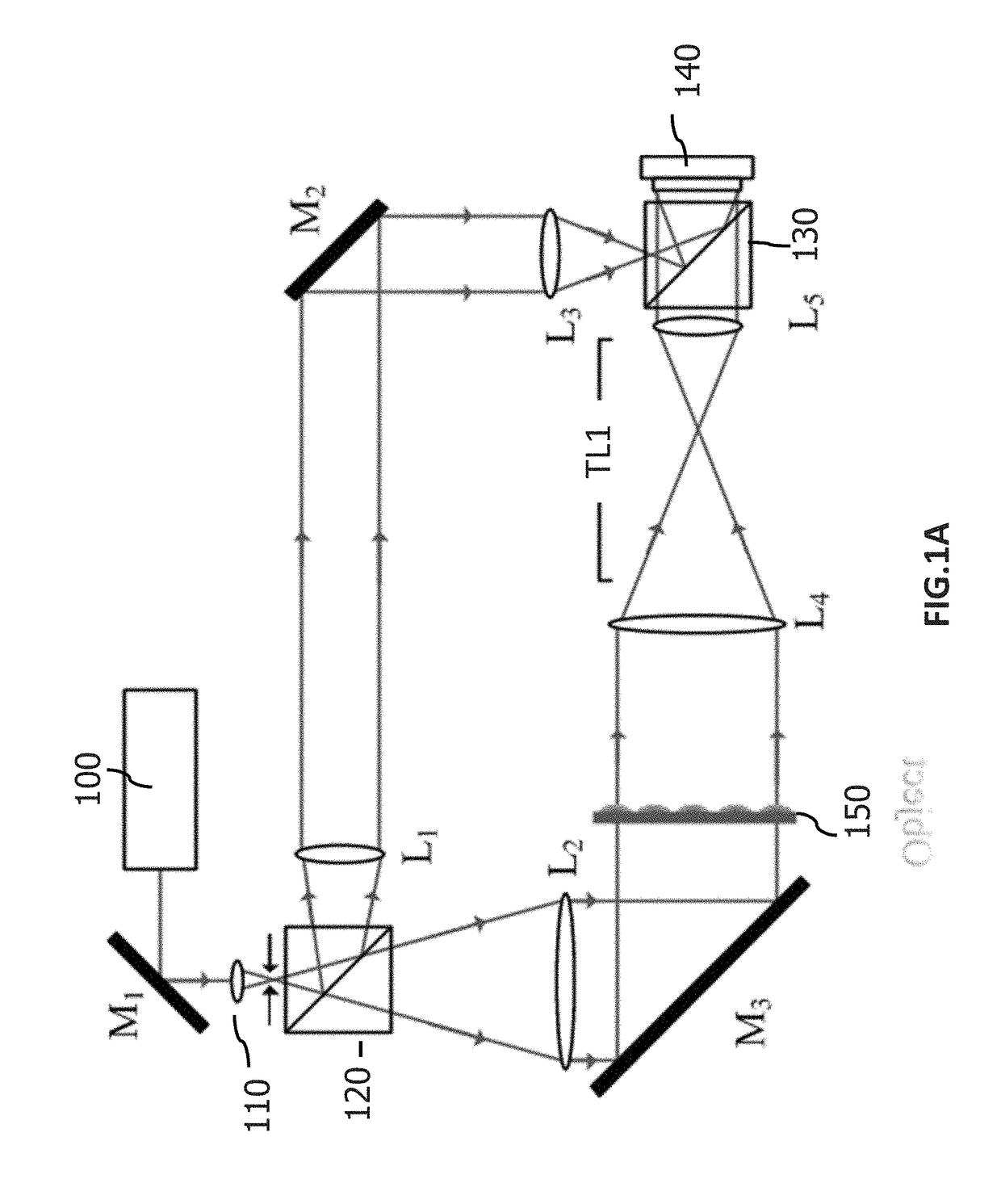
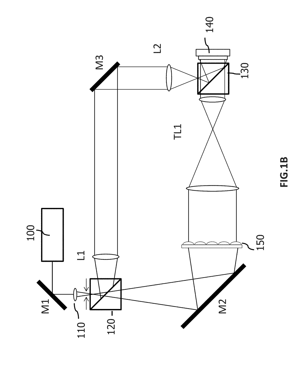
[0052]The invention discloses a method and apparatus by utilizing interference and wavefront recording to reconstruct the defect complex images of a transparent substrate, and characteristics analyzing, features classifying and sieving for the defect complex images of the transparent substrate as reference-based for defect detection. The embodiment indicates a database of defect complex images created by characteristics analysis, features classifying and sieving, to establish a classification u...


PUM


Abstract

A method for defect inspection of a transparent substrate comprises (a) providing an optical system for performing a diffraction process of object wave passing through a transparent substrate, (b) interfering and wavefront recording for the diffracted object wave and a reference wave to reconstruct the defect complex images (including amplitude and phase) of the transparent substrate, (c) characteristics analyzing, features classifying and sieving for the defect complex images of the transparent substrate, and (d) creating defect complex images database based-on the defect complex images for comparison and detection of the defect complex images of the transparent substrate.

Description

TECHNICAL FIELD[0001]The present invention relates to defect inspection of a transparent substrate, and more particularly, to a method and apparatus for inspection of defect complex images by integrating interference and wavefront recording to reconstruct the defect complex images information.BACKGROUND[0002]Glass substrate is one of the most popular and widely components applied for all kinds of optoelectronic products, such as photoelectric display, intelligent mobile phone panel, micro lens and so on. There are a lot of requirements and applications of glass substrate in the field of optoelectronic industry. Especially, in manufacturing and assembling of photovoltaic products including photoelectric display (for example: liquid crystal display, plasma display panel, organic light emitting diode), digital camera, intelligent mobile phone panel, the glass substrate plays a very significant and key role. In addition, in bonding with silicon chip, microelectromechanical systems (MEMS...

Claims


Application Information

Patent Timeline
Patent Type & Authority Applications(United States)
IPC IPC(8): G01B9/021G01B9/02G03H1/04G03H1/16
CPCG01B9/021G01B9/0201G01B9/02016G01B9/02018G03H2001/0212G03H1/0404G03H1/16G03H2001/0216G01B9/0203G03H2223/52G03H2001/0033G03H2001/0447G03H2001/0456G03H2210/12G03H2223/55G03H1/0443G03H2223/12
Inventor CHENG, CHAU-JERNLIU, CHIN-YULAI, XIN-JI
Owner NATIONAL TAIWAN NORMAL UNIVERSITY
Why Eureka
Try Eureka