Semiconductor LED Display Devices

a technology of led display and semiconductors, applied in semiconductor devices, instruments, electrical appliances, etc., can solve the problems of low resolution of colorful display panels (300 ppi), difficult to achieve full-color display, and large pixel pitch, and achieve high contrast, reduced lateral light spreading of micro-led emission, and high resolution

Inactive Publication Date: 2018-07-05
XU FANG +1
View PDF5 Cites 41 Cited by
  • Summary
  • Abstract
  • Description
  • Claims
  • Application Information

AI Technical Summary

Benefits of technology

[0010]The invention described in this disclosure overcomes some existing problems of III-nitride LED displays by achieving, on the same III-nitride display device, high density array of micro-LEDs that are monolithically integrated, reduced lateral light spreading of the micro-LED emission in the color conversion layer, latched storage of video signals, vertical current transport in micro-LEDs, and uniform micro-LED emission across the array. Those features lead to a full-color display device of high resolution, high contrast, improved uniformity and high efficiency.

Problems solved by technology

Currently, one of the major hurdles along the roadmap of III-Nitride micro-LED display development is the difficulty of achieving full-color display.
This arises from the challenges of fabricating, on a single substrate, high-quality red, green and blue LED devices from the same epitaxial LED heterostructure.
There remain a number of drawbacks for those existing III-Nitride LED colorful display technologies which largely arise from the structural configuration of the display devices employed to date: In the first aforementioned technology category, the LED dies or chips constituting the display panel are physically separated from each other although they are assembled and anchored on the same backplane board or silicon substrate for active matrix addressing and driving.
It is difficult to reduce the separating distance (≥10 μm) between those neighboring discrete devices, leading to large pixel pitch and hence low resolution of the colorful display panels (≤300 ppi) demonstrated to date.
Nevertheless, the presence of the LED substrate in the display device configuration has resulted in two problems: first, the color conversion phosphor cells are separated from the emission region of the micro-LEDs by the relatively thick substrate (≥80 μm).
This causes significant crosstalk between the neighboring display pixels and pose severe limitations to the display resolution (≤500 ppi) , as analyzed in the detailed description section of this patent disclosure.
Secondly, the common LED substrate, such as sapphire, for III-nitride devices is insulating, entailing the lateral current flow in the micro-LEDs, which leads to high working voltage and hence low efficiency and non-uniform operation of the pixelated micro-LED emitters.
The charge leakage of those capacitors leads to the shift of the gate bias of the driving transistors and hence the variation of the current flow in the micro-LED loads.
The micro-LED brightness fluctuates accordingly, causing the inaccuracy of the pixel grey-levels in the display.

Method used


Image

  • Semiconductor LED Display Devices
  • Semiconductor LED Display Devices
  • Semiconductor LED Display Devices

Examples


Embodiment Construction

[0020]Embodiments of the present invention relates to semiconductor display devices. More particular embodiments of the present invention relate to a full-color display device based on III-nitride semiconductors. The present invention is designed to addresses some existing problems of III-nitride LED displays, including the low resolution due to pixel pitch size and light spreading in the color conversion layer, non-uniform emission across the array of display pixels, low power efficiency, and limited gray scale.

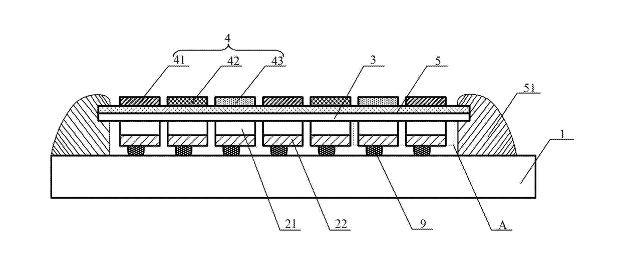
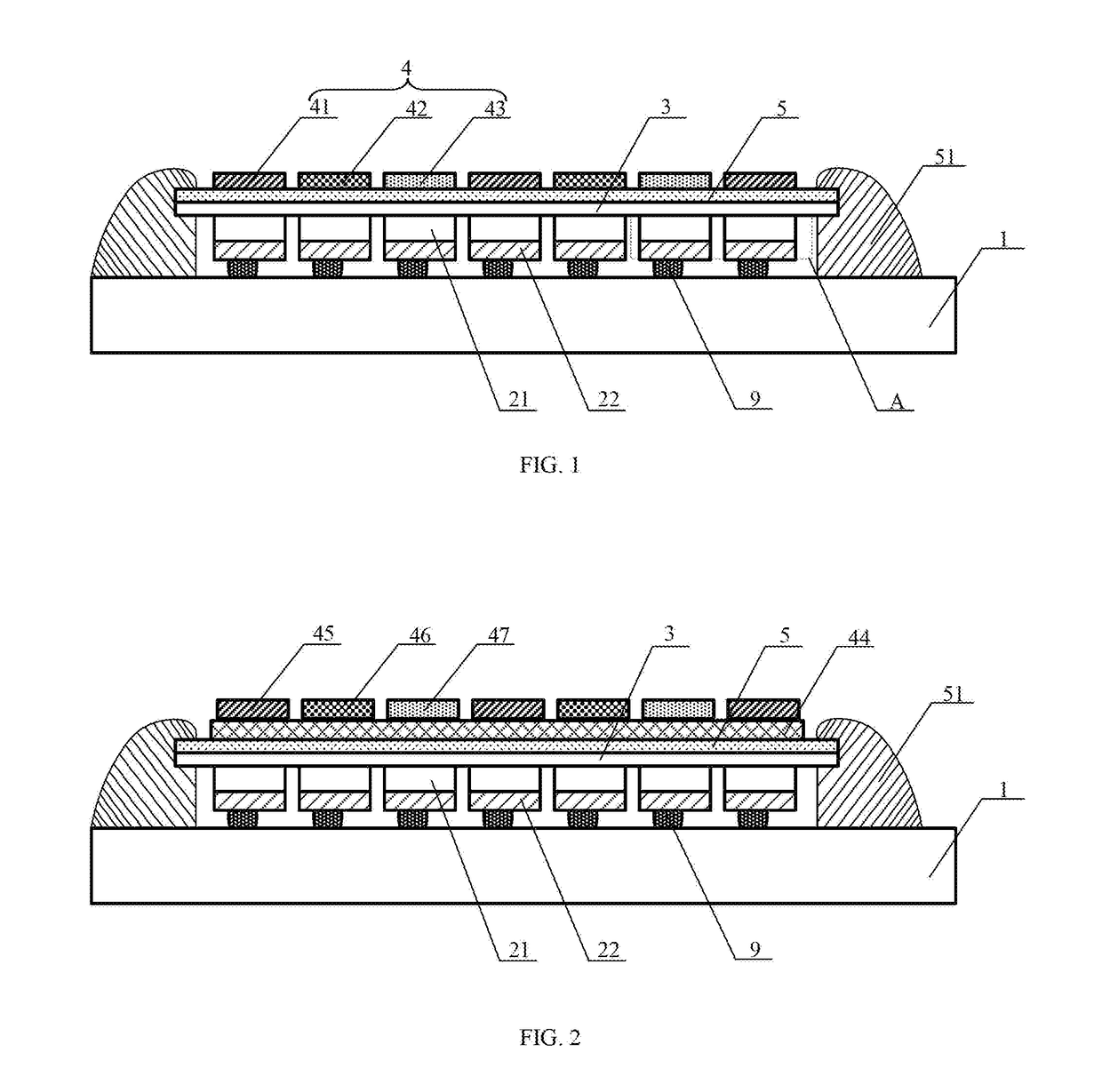
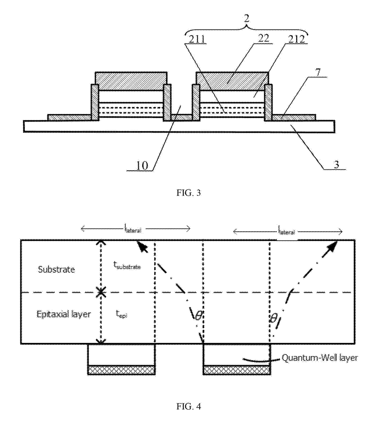
[0021]According to one aspect of the present invention, the full-color LED display device, as illustrated in FIGS. 1-6, comprises an array of micro-LEDs that are monolithically integrated on the single chip of an epitaxially grown III-nitride LED heterostructure, and a silicon backplane 1 of active matrix circuits. The active matrix circuits include a plurality of addressing and driving pixels 11. The substrate of the LED chip shared by the micro-LEDs 2 in the array is remov...


PUM


Abstract

The subject of this invention is a full-color display device based on III-Nitride semiconductors. The display device includes an array of micro-LEDs, monolithically integrated on a single chip of the epitaxially grown LED heterostructure, and flip-chip bonded to a silicon backplane of active matrix driving circuits, and color conversion layers. The LED substrate of the micro-LED array is removed, and the n-regions of the p-n or p-i-n heterojunctions of the micro-LEDs are connected via a thin n-type III-nitride epitaxial layer less than 20 μm thick. The surface of the thin n-type III-nitride epitaxial layer is covered with a layer of transparent/semi-transparent conductive material, forming the common n-type electrode of the micro-LED devices, rendering the vertical current flow in the micro-LED emitters. Each addressing and driving pixel of the active matrix driving circuits contains at least a switching transistor, a switching-driving transistor, and a latch register.

Description

BACKGROUND OF THE INVENTION[0001]Embodiments of the present invention relates to semiconductor display devices. More particular embodiments of the present invention relate to a full-color display device based on III-nitride semiconductors.[0002]In recent years, advances in III-Nitride semiconductor crystal growth and device processing have led to a series of breakthroughs in high-efficiency and high-power LED manufacturing, high-performance packaging, as well as the continuous reduction of the production costs. It has been predicted that the III-Nitride micro-LED-based display technology will outperform the liquid-crystal-on-silicon (LCOS) and Organic-LED (OLED) display technologies by virtue of the superior optical, electrical and mechanical properties of III-Nitride crystalline semiconductors. Currently, one of the major hurdles along the roadmap of III-Nitride micro-LED display development is the difficulty of achieving full-color display. This arises from the challenges of fabri...

Claims


Application Information

Patent Timeline
Patent Type & Authority Applications(United States)
IPC IPC(8): H01L27/15H01L25/16H01L33/62H01L33/00H01L33/32H01L33/50H01L33/42H01L33/12H01L33/06
CPCH01L27/156H01L25/167H01L33/62H01L33/0079H01L33/06H01L33/32H01L33/502H01L33/42H01L33/12H01L33/0012G09G3/32H01L21/77H01L27/12H01L33/504H01L33/507H01L33/0093Y02B20/30
Inventor XU, FANGZHANG, XIJUAN
Owner XU FANG
Why Eureka
Try Eureka