Lateral gallium nitride jfet with controlled doping profile

a gallium nitride and lateral gan junction technology, applied in the field of lateral gan junction field effect transistors (fet), can solve the problems of limited control of junction field effects and breakdown in the channel region between the gate and the drain electrode, and achieve the effects of reducing the electric field, increasing the breakdown voltage, and eliminating the field pla

Active Publication Date: 2018-08-02
QROMIS INC
View PDF0 Cites 10 Cited by
  • Summary
  • Abstract
  • Description
  • Claims
  • Application Information

AI Technical Summary

Benefits of technology

[0004]Embodiments of the present disclosure provide a lateral junction field-effect transistor that has a controlled doping profile that can reduce the electric field and increase the breakdown voltage. One advantage of the present disclosure is to keep the maximum electric field away from the surface of the transistor so that the surface passivation and the field plate can be reduced or eliminated.

Problems solved by technology

Such a large electric field may result in a breakdown in the channel region between the gate and the drain electrode.
One disadvantage of a high-electron mobility transistor (HEMT) is its limited ability to controlling junction field effects.

Method used


Image

  • Lateral gallium nitride jfet with controlled doping profile
  • Lateral gallium nitride jfet with controlled doping profile
  • Lateral gallium nitride jfet with controlled doping profile

Examples


Embodiment Construction

[0022]Embodiments of the present disclosure will be described more fully hereinafter with reference to the accompanying drawings. The invention may, however, be embodied in many different forms and should not be construed as limited to the embodiments set forth herein. Rather, these embodiments are provided so that this disclosure will be thorough and complete, and will fully convey the scope of the invention to those skilled in the art. The features may not be drawn to scale, some details may be exaggerated relative to other elements for clarity. Like numbers refer to like elements throughout.

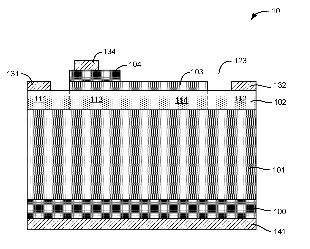
[0023]FIG. 1 is a cross-sectional view illustrating a gallium nitride (GaN) lateral junction field-effect transistor 10 according to one embodiment of the present disclosure. Referring to FIG. 1, lateral junction field-effect transistor (LJFET) 10 includes a substrate 100 of a first conductivity type having a high dopant concentration. For example, substrate 100 is a GaN substrate having a hig...


PUM


Abstract

A lateral junction field-effect transistor includes a substrate of a first conductivity type having a dopant concentration; a first semiconductor layer of the first conductivity type having a first dopant concentration lower than the dopant concentration and disposed on the substrate; a second semiconductor layer of a second conductivity type having a second dopant concentration, the second conductivity type being different from the first conductivity type, the second semiconductor layer disposed on the first semiconductor layer; a third semiconductor layer of the first conductivity type having a third dopant concentration, the third semiconductor layer disposed on the second semiconductor layer; a fourth semiconductor layer of the first conductivity type having a fourth dopant concentration lower than the dopant concentration, the fourth semiconductor layer disposed on the third semiconductor layer; a source region and a drain region disposed in the second semiconductor layer and on opposite sides of the third semiconductor layer.

Description

CROSS-REFERENCES TO RELATED APPLICATIONS[0001]This application claims the benefit of U.S. Provisional Patent Application No. 62 / 452,272, filed on Jan. 30, 2017, the contents of which is incorporated by reference in its entirety.FIELD OF THE INVENTION[0002]The present invention relates to semiconductor technology, and more particularly to a lateral GaN junction field-effect transistor (FET) and the method of forming the same.BACKGROUND OF THE INVENTION[0003]For a power FET, the gate junction is usually biased at a high voltage in order to obtain high output power. In this case, a large electric field is formed in the channel below the gate edge on the drain side. Such a large electric field may result in a breakdown in the channel region between the gate and the drain electrode. One disadvantage of a high-electron mobility transistor (HEMT) is its limited ability to controlling junction field effects.SUMMARY OF THE INVENTION[0004]Embodiments of the present disclosure provide a latera...

Claims


Application Information

Patent Timeline
Patent Type & Authority Applications(United States)
IPC IPC(8): H01L29/808H01L29/20H01L29/66H01L29/08H01L29/417H01L29/423H01L29/06
CPCH01L29/808H01L29/2003H01L29/66893H01L29/0847H01L29/41775H01L29/42312H01L29/0615H01L29/0649H01L29/1058H01L29/1066H01L29/12H01L29/36H01L29/66446
Inventor ODNOBLYUDOV, VLADIMIRAKTAS, OZGUR
Owner QROMIS INC
Why Eureka
Try Eureka